
 中文
中文 English
4-Bit Bidirectional Voltage Level Translator for Open Drain and Push-Pull Applications CXCO4335 is a qual bidirectional I2 C and SMBUS voltage-level translator with an output enable (OE) input, and is
目录
产品概述 返回TOP
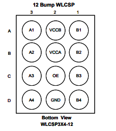
The CXCO4335 is a qual bidirectional I2 C and SMBUS voltage-level translator with an output enable (OE) input, and is operational from 1.2V to 3.3V VCCA and 2.5V to 5.5V VCCB. It allows bidirectional voltage translations between 1.2V and 5V, without use of directional pin. The low ON-state resistance (rON) of the switch ensures the connections to be with minimal propagation delay. When OE is high, the translator switch is ON, and the AN I/O are connected to the BN I/O, respectively, allowing bidirectional data flow between ports. When OE is low, the translator switch is off, and a high-impedance exists between ports. Pull-up resistors are included on input and output lines internally to provide the logic high levels on the translator’s bus. The size of the pull-up resistors are 10kΩ, and is allowed to use lower pull-up resistor value to minimal 1kΩ by adding external resistor. All channels have the same electrical characteristics, and there is minimal deviation from one output to another in voltage or propagation delay. This is a benefit over discrete translation solutions, since the fabrication of the switch is symmetrical.
产品特点 返回TOP
„ 4-Bit Bidirectional Translator for Open Drain and Push-Pull Bus Applications
„ I 2 C and SMBus Compatible
„ Less than 1.5ns Maximum Propagation Delay to Accommodate Standard-Mode and Fast-Model I 2 C Devices and Multiple Masters
„ Allows Voltage-Level Translator Between
Š 1.8V VCCA and 2.5V, 3.3V, 5V VCCB
Š 2.5V VCCA and 3.3V, 5V VCCB
Š 3.3V VCCA and 5V VCCB
Š VCCA ≦ VCCB
„ Provides Bidirectional Voltage Translation without Direction Pin
„ Max Data Rates
Š 24Mbps for Push Pull
Š Over 1.3Mbps for Open Drain
„ Low 3.5Ω ON-State Connection Between Input and Output Ports Provides Less Signal Distortion
„ Open-Drain I2 C I/O Ports
„ 5V Tolerant I2 C I/O Ports to Support Mixed Mode Signal Operation „ High Impedance AN and BN Pins for OE=Low
„ Lock-up-Free Operation for Isolation When OE=Low
„ IEC 61000-4-2 Level 4 (±8kV Contact Discharge and ±15kV Air-gap Discharge) ESD Protection for pins B1, B2, B3, B4, OE and VCCB. 2kV HBM IEC61340-3-1 Protection for All Other Pins.
应用范围 返回TOP
a
技术规格书(产品PDF) 返回TOP
需要详细的PDF规格书请扫一扫微信联系我们,还可以获得免费样品以及技术支持!

a
相关芯片选择指南 返回TOP 更多同类产品。。。。。。
|
Level Shifter |
|||||||||
|
Part NO. |
VDD(V min. |
VDD(V max. |
CH |
IOUT (mA) |
VLOW (V) |
VHIGH (V) |
S/R (ns) |
Note |
Package |
|
6 |
16 |
5 |
50 |
0 |
18 |
25 |
2 Vcom buffers |
TQFN5X5-32 |
|
|
-- |
-- |
8 |
500 |
-35 |
35 |
12 |
VGH1-VGL 6-CH,VGH2-VGL 2-CH |
TSSOP20/TQFN4X4-20 |
|

发表评论