 中文
中文 English
固定300kHz开关率频CXSD6273同步buck-PWM线性控制器0.8V参考输出电压以及监控和保护功能于一体。固定300kHz开关
目录
1.产品概述 2.产品特点3.应用范围 4.下载产品资料PDF文档
5.产品封装图 6.电路原理图
7.功能概述 8.相关产品
一,产品概述(General Description)
The CXSD6273 integrates synchronous buck PWM, linear controller, and 0.8V Reference
Out Voltage, as well as the monitoring and protection functions into a single package. The
fixed 300kHz switching frequency synchro-nous PWM controller drives dual N-channel
MOSFETs,which provides one controlled power output with over-voltage and over-current
protections. Linear controller drives an external N-channel MOSFET with under-volt-
age protection.
The CXSD6273 provides excellent regulation for output load variation. An internal 0.8V
temperature-compensated ref-erence voltage is designed to meet the requirement of
low output voltage applications.
The CXSD6273 with excellent protection functions: POR,OCP, OVP and UVP. The
Power-On-Reset (POR) circuit can monitor VCC12 supply voltage exceeds its threshold
voltage while the controller is running, and a built-in digi-tal soft-start provides both outputs
with controlled rising voltage. The Over-Current Protection (OCP) monitors the output current
by using the voltage drop across the lower MOSFET’s RDS(ON), comparing with the voltage
of OCSET pin, VOCSET. The maximum VOCSET voltage is limited to the internal default value
0.25V. In addition, when OCSET pin is floating (no ROCSET resistor), the over current threshold
will also be internal default value, 0.25V. When the output current reaches the trip point, the
controller will shutdown the IC directly, and latch the converter’s output. The Un-der-Voltage Protection (UVP) monitors the voltage of FBL pin for short-circuit protection. When the VFBL is less than
50% of VREF, the controller will shutdown the IC directly.The Over-Voltage Protection (OVP)
monitors the voltage of FB. When the VFB is over 135% of VREF, the controller will
make Low-side gate signal fully turn on until the fault events are removed.
二.产品特点(Features)
1.)Two Regulated Voltages and REF_OUT Synchronous Buck Converter
Linear Regulator
REF_OUT = 0.8V±1% with 3mA Source Current
2.)Single 12V Power Supply Required
3.)Excellent Both Output Voltage Regulation
0.8V Internal Reference
±1% Over Line Voltage and Temperature
4.)Integrated Soft-Start for PWM and Linear Outputs
5.)300KHz Fixed Switching Frequency
6.)Voltage Mode PWM Control Design and Up to 89%(Typ.) Duty Cycle
7.)Under-Voltage Protection Monitoring Linear Out-put
8.)Over-Voltage Protection Monitoring PWM Output
9.)Over-Current Protection for PWM Output Sense Low-side MOSFET’s RDS(ON)
10.)SOP-14, SSOP-16 and Compact QFN4x4-16 pack-ages
11.)Lead Free and Green Devices Available(RoHS Compliant)
三,应用范围 (Applications)
Graphic Cards
四.下载产品资料PDF文档
需要详细的PDF规格书请扫一扫微信联系我们,还可以获得免费样品以及技术支持!

五,产品封装图 (Package)
FUNCTION NAMEFUNCTION
|
PIN NO. |
NAME |
FUNCTION |
||
|
SOP-14 |
SSOP-16 |
QFN4x4-16 |
||
|
1 |
15 |
BOOT |
This pin provides the bootstrap voltage to the upper gate driver for driving the N-channel MOSFET. An external capacitor from PHASE to BOOT, an internaldiode, and the power supply voltage VCC12, generates the bootstrap voltage |
|
|
2 |
2 |
16 |
FS_DIS |
This pin provides shutdown function. When pulling low the FS_DIS pin near GND will shutdown both regulators; almost any NFET or other pull-down device (< 1k. impedance) should work. Upon release of the FS_DIS pin, it will |
|
3 |
3 |
1 |
COMP |
This pin is the output of PWM error amplifier. It is used to set the compensation components. |
|
4 |
4 |
2 |
FB |
This pin is the inverting input of the PWM error amplifier. It is used to set the output voltage and the compensation components. This pin is also monitored |
|
5 |
5 |
3 |
DRIVE |
This pin drives the gate of an external N-channel MOSFET for linear regulator. |
|
6 |
6 |
4 |
FBL |
This pin is the inverting input of the linear regulator error amplifier. It is used to |
|
7 |
7,8 |
5,6 |
GND |
This pin is the signal ground pin. Connect the GND pin to a good ground plane. |
|
8 |
9,10 |
7,8 |
VCC12 |
Power supply input pin. Connect a nominal 12V power supply to this pin. Thepower- on reset function monitors the input voltage at this pin. It is recommended that a decoupling capacitor (1 to 10μF) be connected to GND for noise decoupling. |
|
9 |
11 |
9 |
REF_OUT |
This pin provides a buffed voltage, which is from internal reference voltage. It is recommended that a 1mF capacitor is connected to ground for stability. |
|
10 |
12 |
10 |
OCSET |
Connect a resistor (ROCSET) from this pin to GND, an internal 40mA current source will flow through this resistor and create a voltage drop. When VCC12 reaches the POR rising threshold voltage, the voltage drop of ROCSET will be |
|
11 |
13 |
11 |
LGATE |
This pin is the gate driver for the lower MOSFET of PWM output. |
|
12 |
14 |
12 |
PGND |
This pin is the power ground pin for the lower gate driver. It should be tied to GND pin on the board. |
|
13 |
15 |
13 |
PHASE |
This pin is the return path for the upper gate driver. Connect this pin to the upper MOSFET source, and connect a capacitor to BOOT for the bootstrap voltage. This pin is also used to monitor the voltage drop across the lower |
|
14 |
16 |
14 |
UGATE |
This pin is the gate driver for the upper MOSFET of PWM output. |
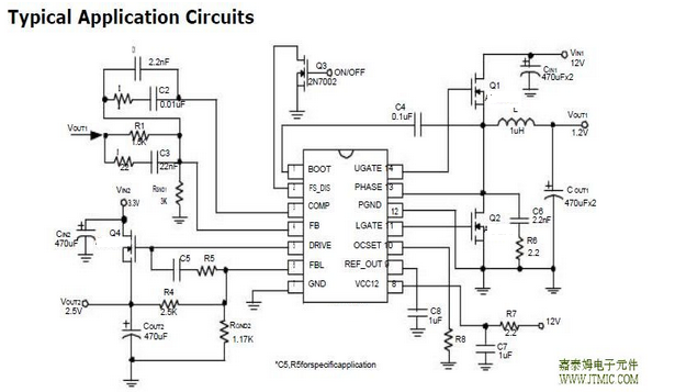
六.电路原理图

七,功能概述
Function Description (Cont.)
Over-Current Protection (Cont.)
When OCSET PIN is floating, the VOCSET will be pulled high and the over current threshold will be the
internal default value 0.25V. When the voltage drop across the lower MOSFET’s RDS(ON) is larger than
0.25V, an over-cur-rent condition is detected, the controller will shutdown the IC directly, and latch
the converter’s output.
Over Voltage Protection
The FB pin is monitored during converter operation by its own Over Voltage(OV) comparator. If the
FB voltage is over 135% of the reference voltage, the controller will make Low-Side gate signal fully
turn on until the fault events are removed.
Under Voltage Protection
The FBL pin is monitored during converter operation by its own Under Voltage (UV) comparator. If
the FBL voltage drop below 50% of the reference voltage (50% of 0.8V =0.4V), a fault signal is
internally generated, and the de-vice turns off both high-side and low-side MOSFET and the
converter’s output is latched to be floating. The con-troller will shutdown the IC directly.
Shutdown and Enable
Pulling low the FS_DIS pin near GND by an open drain transistor or other pull-down device
(<1k. impedance)will shutdown both regulators. Upon release of the FS_DIS pin, it will
enable both outputs back into regulation. In shutdown mode, the UGATE and LGATE
turn off and pull to PHASE and GND respectively.
八,相关产品 更多同类产品......
|
Switching Regulator > Buck Controller |
||||||||||
|
Part_No |
Package |
Archi tectu |
Phase |
No.of PWM Output |
Output Current (A) |
Input Voltage (V) |
Reference Voltage (V) |
Bias Voltage (V) |
Quiescent Current (uA) |
|
|
min |
max |
|||||||||
|
SOP-14 QSOP-16 QFN4x4-16 |
VM |
1 |
1 |
30 |
2.9 |
13.2 |
0.9 |
12 |
8000 |
|
|
SOP-8 |
VM |
1 |
1 |
20 |
2.9 |
13.2 |
0.8 |
12 |
5000 |
|
|
SOP-8 |
VM |
1 |
1 |
20 |
2.9 |
13.2 |
0.8 |
12 |
5000 |
|
|
QFN4x4-24 |
VM |
2 |
1 |
60 |
3.1 |
13.2 |
0.6 |
12 |
5000 |
|
|
SOP-8 |
VM |
1 |
1 |
20 |
2.2 |
13.2 |
0.8 |
5~12 |
2100 |
|
|
SOP-8 |
VM |
1 |
1 |
20 |
2.2 |
13.2 |
0.8 |
5~12 |
2100 |
|
|
SOP8|TSSOP8 |
VM |
1 |
1 |
5 |
5 |
13.2 |
1.25|0.8 |
5~12 |
3000 |
|
|
SOP-8 |
VM |
1 |
1 |
10 |
3.3 |
5.5 |
0.8 |
5 |
2100 |
|
|
SOP-14 |
VM |
1 |
1 |
10 |
5 |
13.2 |
0.8 |
12 |
2000 |
|
|
TSSOP-24 |QFN5x5-32 |
VM |
1 |
2 |
20 |
5 |
13.2 |
0.6 |
5~12 |
4000 |
|
|
SOP14 QSOP16 QFN-16 |
VM |
1 |
1 |
30 |
2.9 |
13.2 |
0.9 |
12 |
4000 |
|
|
SOP-14 |
VM |
1 |
1 |
30 |
2.2 |
13.2 |
0.6 |
12 |
5000 |
|
|
SOP-14 |
VM |
1 |
1 |
30 |
2.2 |
13.2 |
0.6 |
12 |
5000 |
|
|
SOP-14 |
VM |
1 |
1 |
25 |
2.2 |
13.2 |
0.8 |
12 |
5000 |
|
|
LQFP7x7 48 TQFN7x7-48 |
VM |
1 |
6 |
0.015 |
1.4 |
6.5 |
- |
5 |
1800 |
|
|
TSSOP-24P |
VM |
1 |
2 |
20 |
2.97 |
5.5 |
0.8 |
5~12 |
5000 |
|
|
SOP-14 |
VM |
1 |
1 |
10 |
5 |
13.2 |
0.8 |
12 |
3000 |
|
|
SOP-8-P|DIP-8 |
VM |
1 |
1 |
30 |
2.9 |
13.2 |
1.2 |
12 |
3000 |
|
|
SSOP28 QFN4x4-24 |
VM |
1 |
2 |
20 |
5 |
24 |
0.9 |
5</ |
||


发表评论