 中文
中文 English
CXSD6280两个同步降压型脉宽调制控制器高精度内部参考电压的线性控制器PWM控制器同步buck拓扑中的两个N沟道mosfet
目录
1.产品概述 2.产品特点
3.应用范围 4.下载产品资料PDF文档
5.产品封装图 6.电路原理图
7.功能概述 8.相关产品
一,产品概述(General Description)
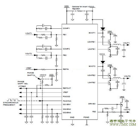
The CXSD6280 has two synchronous buck PWM control-lers
and one linear controller with high precision internal references voltage
to offer accurate outputs. The PWM controllers are designed to drive
two N-channel MOSFETs in synchronous buck topology, and the linear
controller drives an external N-channel MOSFET. The device re-quires
12V and 5V power supplies, if the 5V supply is not available, VCC12 can
offer an optional shunt regulator 5.8V for 5V supply.All outputs have
independent soft-start and enable func-tions by SS/EN pins to control.
Connect a capacitor from each SS/EN pin to the ground for setting the
soft-start time, and pulling the SS/EN pin below 1V to disable regulator.
Pull the SS2/EN2 to VCC, enter the DDR mode,the SS1/EN1 controls
both VOUT1 and VOUT2, and al-lows VOUT2 to track VOUT1. It also
offers the phase shift function by REFOUT pin to select the phase shift
between VOUT1 and VOUT2 in DDR mode or Independent mode.
When all SS/EN pins exceed 3.3V and no faults are detected, the PGOOD
pin goes high to indicate the regu-lators are ready. If any of the SS/EN pins
goes below 3.2V or any of the outputs has a fault condition, the PGOOD pin
will be pulled low.
The internal oscillator is nominally 300kHz (keep the FS/SYNC pin open
or short to GND), and it offers the pro-grammable frequency function from
70kHz to 800kHz; con-necting a resistor from FS/SYNC to VCC12 to decrease
the frequency, conversely, connect a resistor from FS/SYNC to GND to
increase the frequency.The IC also pro-vides the synchronous frequency
function. Connect the LGATE signal of another converter to FS/SYNC pin;
forc-ing the switching frequency to follow the external clock.
The possible synchronous frequency is from 150kHz to 800kHz. There
is no Rds(on) sensing or under-voltage sens-ing on CXSD6280. However, it
provides a simple short-circuit protection by monitoring the COMP1 and COMP2
for over-voltage. When any of two pins exceeds their trip point and the condition
persists for 1-2 internal clock cycle (3-6μs at 300kHz), then it will shut down
all regulators.
二.产品特点(Features)
1.)Two Synchronous Buck Converters and A Linear Regulator
2.)VIN Range up to 12V
3.)Input Power Supplies Require 12V and 5V or
4.)Use 12V to Generate a Shunt Regulator 5.8V
5.)0.6V Reference for VOUT1 and VOUT3 with 0.8% Accurate
6.)3.3V Reference for VOUT2 with 0.8% Accurate
7.)Buffered VTT Reference Output
8.)Three Outputs have Independent Soft-Start and Enable
9.)Internal 300kHz Oscillator and Programmable
10.)Frequency Range from 70 kHz to 800kHz
11.)Synchronous Switching Frequency
12.)DDR Mode or Independent Mode Selection
13.)Phase Shift Selection
14.)Power Good Function
15.)Short-Circuit Protection for VOUT1 and VOUT2
16.)Thermally Enhanced TSSOP-24P and QFN5x5-32 Packages
17.)Lead Free and Green Devices Available (RoHS Compliant)
三,应用范围 (Applications)
Graphic Cards
DDR memory Power Supplies
Low-Voltage Distributed Power Supplies
四.下载产品资料PDF文档
需要详细的PDF规格书请扫一扫微信联系我们,还可以获得免费样品以及技术支持!

五,产品封装图 (Package)

FUNCTIONNAMEFUNCTION
These pins are the outputs of error amplifiers of their respective regulators. They are
used to set the compensation components.
These pins provide two functions. Connect a capacitor to the GND for setting the
soft-start time. Use an open drain logic signal to pull the SS/EN pin low to disable the
respective output, leave open to enable the respective output.
These pins provide two functions. Connect a capacitor to the GND for setting the
soft-start time. Use an open drain logic signal to pull the SS/EN pin low to disable the
respective output, leave open to enable the respective output.
|
PIN |
FUNCTION |
||
|
NO. |
NAME |
||
|
TSSOP-24P |
DFN5x5-32 |
||
|
1 |
29 |
FB1 |
These pins are the inverting inputs of the error amplifiers of their respective regulators. They are used to set the output voltage and the compensation components. |
|
2 |
30 |
COMP1 |
These pins are the outputs of error amplifiers of their respective regulators. They are used to set the compensation components. |
|
3 |
31 |
COMP2 |
|
|
4 |
32 |
FB2 |
These pins are the inverting inputs of the error amplifiers of their respective regulators. They are used to set the output voltage and the compensation components. |
|
5 |
1 |
REFIN |
This pin is the reference input voltage of error amplifier of the VOUT2. It also provides the voltage into a buffer, which is out on the REFOUT pin. |
|
6 |
3 |
REFOUT |
This pin provides a buffed voltage, which is from REFIN pin. In Independent mode, it can be used by other ICs. In DDR mode, it is from the VOUT1, and can be used as the VTT buffer. This pin also uses to select the phase shift (see table1). When this pin |
|
7 |
4 |
SS1/EN1 |
These pins provide two functions. Connect a capacitor to the GND for setting the soft-start time. Use an open drain logic signal to pull the SS/EN pin low to disable the respective output, leave open to enable the respective output. |
|
8 |
5 |
SS2/EN2 |
|
|
9 |
6 |
SS3/EN3 |
|
|
10 |
7 |
VREF |
This pin provides a 3.3V reference voltage, which can be used by the REFIN pin or other ICs as a voltage reference. It is recommended that a 1μF capacitor is connected to ground for stability |
|
11 |
8 |
DRIVE3 |
This pin drives the gate of an external N-channel MOSFET for linear regulator. |
|
12 |
10 |
FB3 |
These pins are the inverting inputs of the error amplifiers of their respective regulators. They are used to set the output voltage and the compensation components. |
|
13 |
11 |
FS/SYNC |
This pin is used to adjust the switching frequency. Connecting a resistor from FS/SYNC pin to the ground increases the switching frequency. Conversely,connecting a resistor from this pin to the VCC12 reduces the switching frequency. In addition, this pin also provides synchronous frequency function. An external clock can be fed into this pin, and force the switching frequency to follow the external clock. |
|
14 |
12 |
PGOOD |
This pin is an open drain device; connect a pull up resistor to the VCC for PGOOD function. |
|
15 |
13 |
GND |
This pin is the signal ground pin. The metal thermal pad under the package is the IC substrate; connects the GND pin and metal thermal pad together on the board, and ties to the good GND plane for electrical and thermal conduction. |
|
16 |
16 |
BOOT2 |
These pins provide the bootstrap voltage to the gate driver for driving the upper MOSFETs. It can be connected to a power voltage directly, but the difference voltage between the BOOT and VIN must be high enough to drive the upper MOSFETs. |
|
17 |
14 |
UGATE2 |
These pins provide the gate driver for the upper MOSFETs of VOUT1 and VOUT2. |
|
18 |
18,23 |
PGND |
This pin is the power ground pin for the gate driver and linear driver circuit. It should be tied to the GND. |
|
19 |
20 |
LGATE2 |
These pins provide the gate driver for the lower MOSFETs of VOUT1 and VOUT2. |
|
20 |
21 |
LGATE1 |
These pins provide the gate driver for the lower MOSFETs of VOUT1 and VOUT2. |
|
21 |
19, 22 |
VCC12 |
Power supply input pin. Connect a nominal 12V power supply to this pin for the gate driver. It is recommended that a decoupling capacitor (1 to 10μF) is connected to the GND for noise decoupling. |
六.电路原理图

七,功能概述
Soft-Start/Enable
The three SS/EN pins control the soft-start and enable or disable the controller. In Independent mode, the three
regulators all have independent soft-start and enable functions. Connect a soft-start capacitor from each SS/EN
pin to the GND to set the soft-start interval, and an open drain logic signal for each SS/EN pin will enable or dis-
able the respective output.
八,相关产品 更多同类产品......
|
Switching Regulator > Buck Controller |
||||||||||
|
Part_No |
Package |
Archi tectu |
Phase |
No.of PWM Output |
Output Current (A) |
Input Voltage (V) |
Reference Voltage (V) |
Bias Voltage (V) |
Quiescent Current (uA) |
|
|
min |
max |
|||||||||
|
SOP-14 QSOP-16 QFN4x4-16 |
VM |
1 |
1 |
30 |
2.9 |
13.2 |
0.9 |
12 |
8000 |
|
|
SOP-8 |
VM |
1 |
1 |
20 |
2.9 |
13.2 |
0.8 |
12 |
5000 |
|
|
SOP-8 |
VM |
1 |
1 |
20 |
2.9 |
13.2 |
0.8 |
12 |
5000 |
|
|
QFN4x4-24 |
VM |
2 |
1 |
60 |
3.1 |
13.2 |
0.6 |
12 |
5000 |
|
|
SOP-8 |
VM |
1 |
1 |
20 |
2.2 |
13.2 |
0.8 |
5~12 |
2100 |
|
|
SOP-8 |
VM |
1 |
1 |
20 |
2.2 |
13.2 |
0.8 |
5~12 |
2100 |
|
|
SOP8|TSSOP8 |
VM |
1 |
1 |
5 |
5 |
13.2 |
1.25|0.8 |
5~12 |
3000 |
|
|
SOP-8 |
VM |
1 |
1 |
10 |
3.3 |
5.5 |
0.8 |
5 |
2100 |
|
|
SOP-14 |
VM |
1 |
1 |
10 |
5 |
13.2 |
0.8 |
12 |
2000 |
|
|
TSSOP-24 |QFN5x5-32 |
VM |
1 |
2 |
20 |
5 |
13.2 |
0.6 |
5~12 |
4000 |
|
|
SOP14 QSOP16 QFN-16 |
VM |
1 |
1 |
30 |
2.9 |
13.2 |
0.9 |
12 |
4000 |
|
|
SOP-14 |
VM |
1 |
||||||||


发表评论