 中文
中文 English
CXSD6288双通道恒定时间和同步的PWM控制器每个通道驱动双N通道MOSFET功率因数调制或脉宽调制模式下瞬态响应和精确的直流电压输出
目录
1.产品概述 2.产品特点
3.应用范围 4.下载产品资料PDF文档
5.产品封装图 6.电路原理图
7.功能概述 8.相关产品
一,产品概述(General Description)
The CXSD6288 is a dual-channel, constant on-time, and
synchronous PWM controller which drives dual N-channel MOSFETs
for each channel. The CXSD6288 steps down high voltage of a battery
to generate low-voltage chipset or RAM supplies in notebook computers.
The CXSD6288 provides excellent transient response and accurate DC voltage output in either PFM or PWM mode. In PFM mode, the TMA7108 provides very high efficiency over light to heavy loads with loading-modu-
lated switching frequencies. The Forced-PWM mode works nearly at constant frequency for low-noise requirements.
The CXSD6288 is equipped with accurate current-limit,output under-voltag, and output over-voltage protections,perfect for NB applications. A Power-On-Reset function monitors the voltage on V CC to prevent wrong opera-tion during power on. A soft-start ramps up the output voltage with programmable slew rate to reduce the start-up current. A soft-stop function actively discharges the output capacitors with controlled reverse inductor current. At the end of the soft-stop, the CXSD6288 forces
LGATE high to prevent over-voltage in shutdown. The CXSD6288 has individual enable controls for each channel. Pulling both EN pin low shuts down the whole chip with low quiescent current close to zero.
The CXSD6288 is available in SSOP-28 and QFN4x4-24 packages.
二.产品特点(Features)
1.)Adjustable Output Voltage up to 5.5V
- 0.9V Reference Voltage
- ±1% Accuracy Over Temperature
2.)Operates from an Input Battery Voltage Range of
3.)5V to 24V or from 3.3V/5V System Rail
4.)Power-On-Reset Monitoring on VCC Pin
Selectable Forced PWM or Automatic PFM/PWM Mode
5.)Constant-On-Time Control Scheme
- Switching Frequency Compensation for PWM Mode
- Constant Switching Frequency (CH1: 345kHz,
CH2: 255KHz) in PWM Mode with DC Output Current
6.)Excellent Line and Load Transient Responses
7.)Adjustable Soft-Start and Soft-Stop
8.)Power-Good Outputs for both Channels
9.)Adjustable Current-Limit Protection
- Using Sense Resistor or MOSFET’s RDS(ON)
10.)115% Over-Voltage Protection
- No Negative Output Voltage Occurred
11.)70% Under-Voltage Protection
12.)Adaptive Dead-Time Control
- Sensing G-to-S Voltage of Power MOSFETs
13.)Shutdown Control for both Channels
14.)28-pin SSOP (SSOP-28) and 4mmx4mm 24-lead
QFN (QFN4x4-24) Packages
15.)Lead Free and Green Devices Available
三,应用范围 (Applications)
Note Book Computers
- Chipset/RAM Supplies as low as 0.9V
- 1.8V and 2.5V Supplies
Step-Down Converters Requiring High Efficiency
四.下载产品资料PDF文档
需要详细的PDF规格书请扫一扫微信联系我们,还可以获得免费样品以及技术支持!

五,产品封装图 (Package)

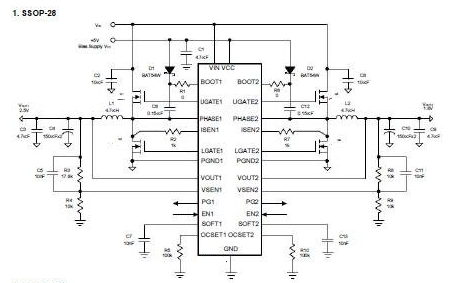
六.电路原理图


七,功能概述
Layout Consideration (Cont.)
· Keep the switching nodes (UGATEx, LGATEx, BOOTx,PHASEx, and ISENx) away from sensitive small sig-
nal nodes since these nodes are fast moving signals.Therefore, keep traces to these nodes as short as
possible and there should be no other weak signal traces in parallel with theses traces on any layer.
· The signals going through theses traces have both high dv/dt and high di/dt, with high peak charging and
discharging current. The traces from the gate drivers to the MOSFETs (UGATEx and LGATEx) should be short
and wide.
· Place the source of the high-side MOSFET and the drain of the low-side MOSFET as close as possible.
Minimizing the impedance with wide layout plane between the two pads reduces the voltage bounce of
the node.
· The ISENx trace should be a separate trace, and independently go to the drain terminal of the low-side
MOSFET. The current sense resistor should be close to ISENx pin. The loop formed by the bottom MOSFET,
output inductor, and output capacitor, should be very small. The source of the bottom MOSFET should tie
to the negative side of the output capacitor in order for the ISENx pin to get the voltage drop on the RDS(ON).
· Decoupling capacitor, compensation component,the resistor dividers, boot capacitors, and soft-start
capacitors should be close their pins. (For example,place the decoupling ceramic capacitor near the drain
of the high-side MOSFET as close as possible. The bulk capacitors are also placed near the drain).
· The input capacitor should be near the drain of the high-side MOSFET; the high quality ceramic
decoupling capacitor can be put close to the VCC and GND pins; the output capacitor should be near the
loads. The input capacitor GND should be close to the output capacitor GND and the low-side MOSFET
GND.
· The drain of the MOSFETs (VIN and PHASEx nodes) should be a large plane for heat sinking. And
PHASEx pin traces are also the return path for UGATEx. Connect these pins to the respective
converter’s high-side MOSFET source.
The CXSD6288 uses ripple mode control. Build the resistor divider close to the VSENx pin so that the
high impedance trace is shorter. The VSENx pin traces can’t be closed to the switching signal traces (UGATEx,
LGATEx, BOOTx, PHASEx, and ISENx).
The PGNDx trace should be a seperate trace, and inpendently go to the source of the low-side MOSFET.
For QFN4x4-24 package only, the thermal pad is the PGND of the dual channels. The sources of the both
channels’ low-side MOSFETs should be near the PGND respectively.
八,相关产品 更多同类产品......
|
Switching Regulator > Buck Controller |
||||||||||
|
Part_No |
Package |
Archi tectu |
Phase |
No.of PWM Output |
Output Current (A) |
Input Voltage (V) |
Reference Voltage (V) |
Bias Voltage (V) |
Quiescent Current (uA) |
|
|
min |
max |
|||||||||
|
SOP-14 QSOP-16 QFN4x4-16 |
VM |
1 |
1 |
30 |
2.9 |
13.2 |
0.9 |
12 |
8000 |
|
|
SOP-8 |
VM |
1 |
1 |
20 |
2.9 |
13.2 |
0.8 |
12 |
5000 |
|
|
SOP-8 |
VM |
1 |
1 |
20 |
2.9 |
13.2 |
0.8 |
12 |
5000 |
|
|
QFN4x4-24 |
VM |
2 |
1 |
60 |
3.1 |
13.2 |
0.6 |
12 |
5000 |
|
|
SOP-8 |
VM |
1 |
1 |
20 |
2.2 |
13.2 |
0.8 |
5~12 |
2100 |
|
|
SOP-8 |
VM |
1 |
1 |
20 |
2.2 |
13.2 |
0.8 |
5~12 |
2100 |
|
|
SOP8|TSSOP8 |
VM |
1 |
1 |
5 |
5 |
13.2 |
1.25|0.8 |
5~12 |
3000 |
|
|
SOP-8 |
VM |
1 |
1 |
10 |
3.3 |
5.5 |
0.8 |
5 |
2100 |
|
|
SOP-14 |
VM |
1 |
1 |
10 |
5 |
13.2 |
0.8 |
12 |
2000 |
|
|
TSSOP-24 |QFN5x5-32 |
VM |
1 |
2 |
20 |
5 |
13.2 |
0.6 |
5~12 |
4000 |
|
|
SOP14 QSOP16 QFN-16 |
VM |
1 |
1 |
30 |
2.9 |
13.2 |
0.9 |
12 |
4000 |
|
|
SOP-14 |
VM |
1 |
1 |
30 |
2.2 |
13.2 |
0.6 |
12 |
5000 |
|
|
SOP-14 |
VM |
1 |
1 |
30 |
2.2 |
13.2 |
0.6 |
12 |
5000 |
|
|
SOP-14 |
VM |
1 |
1 |
25 |
2.2 |
13.2 |
0.8 |
12 |
5000 |
|
|
LQFP7x7 48 TQFN7x7-48 |
VM |
1 |
6 |
0.015 |
1.4 |
6.5 |
- |
5 |
1800 |
|
|
TSSOP-24P |
VM |
1 |
2 |
20 |
2.97 |
5.5 |
0.8 |
5~12 |
5000 |
|
|
SOP-14 |
VM |
1 |
1 |
10 |
5 |
13.2 |
0.8 |
12 |
3000 |
|
|
SOP-8-P|DIP-8 |
VM |
1 |
1 |
30 |
2.9 |
13.2 |
1.2 |
12 |
3000 |
|
|
SSOP28 QFN4x4-24 |
VM |
1 |
2 |
20 |
5 |
|||||


发表评论