 中文
中文 English
CXSD6108 is high efficiency synchronous,PWM step-down DC/DC converters working under an input voltage range from 2.2V to 5.5V. This feature makes CXSD6108 suitable for single Li-Lon battery-p
目录
1.产品概述 2.产品特点
3.应用范围 4.下载产品资料PDF文档
5.产品封装图</span> 6.电路原理图</span>
7.功能概述 8.相关产品
一,产品概述(General Description) ![]()
The CXSD6108 is high efficiency synchronous,PWM step-down DC/DC converters working under an input voltage range from 2.2V to 5.5V.
This feature makes the CXSD6108 suitable for single Li-Lon battery-powered applications. 100% duty cycle capability extends battery life in portable
devices, while the quiescent current is 200μA with no load, and drops to<1μA
in shutdown.
The internal synchronous switch is desired to increase efficiency without an external Schottky diode. The 1.0MHz/1.4MHz switching frequency allows the
using of tiny, low profile inductors and ceramic capacitors, which minimized
overall solution footprint.
The CXSD6108 converters are available in the industry standard TSOT/
SOT-23-5L power packages (or upon request)
二</span>.产品特点(Features)![]()
Up to 95% Efficiency
Current Mode Operation for Excellent Line
and Load Transient Response
700mA Output Current
Low Quiescent Current: 200μA
Output Voltage: 0.6V ~ 5.5V
Automatic PWM/PFM Mode Switching
No Schottky Diode Required
Frequency Operation: 1.0MHz for Fixed
Output Voltage and 1.4MHz for Adjustable
Output Voltage
Short-Circuit Protection
Shutdown Quiescent Current:<1μA
Low Profile TSOT/ SOT-23-5L Package
(lead-free packaging is now available)
三,应用范围 (Applications)![]()
Digital cameras and MP3
Palmtop computers / PDAs
Cellular phones
Wireless handsets and DSL modems
Portable media players
PC cards
四.技术</span>规格书下载(产品PDF)</span>
需要详细的PDF规格书请扫一扫微信联系我们,还可以获得免费样品以及技术支持</span>!</span>

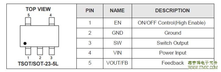
五,产品封装图 (Package)![]()
六.电路原理图</span>![]()

七</span>,功能概述![]()
Power Dissipation………………………………………………………………………Internally Iimited
Input Voltage…………………………………………………………………………………..-0.3V ~ +6V
Output Voltage……………………………………………………………………….…….....-0.3V ~ +6V
EN,SW Pin Voltage……………………..………………..……………………...……-0.3V ~ (VIN+0.3)V
SW Pin Current….………………………………………………………………...……………………..1.3A
Operating Temperature Range(Note 2) ………………………………………………...-40℃ ~ +85℃</span>
Junction Temperature ………………………………………………………...…………-40℃ ~ +125℃</span>
Storage Temperature Range ………………………………………………………….-65℃ ~ +150℃</span>
Lead Temperature (Soldering,10 sec.) ………………………………………..…………………..+265℃</span>
八,相关芯片选择指南 更多同类产品......![]()
DC-DC降压 | |||||
Model | VIN (V) | VOUT (V) | ISW | FOSC(MHz) | Package |
0.6V ~5V | 0.6 ~ 5.5 | 1.3A | 1~1.4 | SOT-23-5L | |
5V~16V | 1.2V~16V | 2A | 400kHz | SOP-8L | |
2.5 ~ 5.5 | 0.6 ~ 5.5 | 1.3A | 1~1.4 | SOT-23-5L | |
2.5 ~ 5.5 | 0.6V ~ 5.5V | 700mA | 1.4MHz | DFN3*3-10L | |
2.5V ~5.5V | 0.6V ~ 5.5V | 3A | 950kHz | SOT-23-5L | |
2.5V ~5.5V | 0.6V ~ 5.5V | 1.4A | 950kHz | SOT-23-5L | |
10V ~ 30V | 0.6V ~ 5.5V | 2.5A | 500k | SOP-8 | |
8V ~ 30V | 0.6V ~ 5.5V | 3.5A | 500KHz | SOP8 | |
8V ~ 30V | 0.6V ~ 5.5V | 3.0A | 500KHz | SOP8 | |
8V ~ 30V | 0.6V ~ 5.5V | 2A | 500KHz | SOP8 | |

发表评论