 中文
中文 English
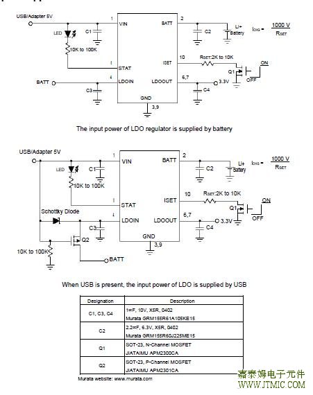
The JTMA3207 combines a constant-current/constant-volt-age linear single cell Li+ battery charger with a low drop-out linear regulator. Both charger and linear regulators can work independently. The
摘要:The JTMA3207 combines a constant-current/constant-volt-age linear single cell Li+ battery charger with a low drop-out linear regulator. Both charger and linear regulators can work independently. The
目录
一,产品概述(General Description)
The JTMA3207 combines a constant-current/constant-volt-age linear single cell Li+ battery charger with a low drop-out linear regulator. Both charger and linear regulators can work independently. The small DFN-10 package and low external component count make the JTMA3207 ideally
suit to portable applications.
The charger of JTMA3207 provides 0.7A charge currentwith thermal regulation protection to optimize the board design for compact size and typical thermal conditions.When the junction temperature reaches the thermal regu-lation threshold, the charger does not shut down but sim-
ply reduces the charge current. The charge current can be programmed by connecting an external resistor from the ISET pin to the GND. Using an external MOSFET to disconnect the resistor from the ground shuts down the charger, and reduces the input current down to 25μA.
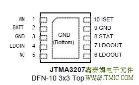
The JTMA3207 also has the STAT pin to indicate charge status.
The LDO regulator of JTMA3207 can deliver up to 150mA current and dropout voltage is only 200mV. The 4μA low quiescent current makes it ideally suit to battery-power systems. The LDO regulator also has built-in current limit and thermal shutdown protection.
二</span>.产品特点(Features)suit to portable applications.
The charger of JTMA3207 provides 0.7A charge currentwith thermal regulation protection to optimize the board design for compact size and typical thermal conditions.When the junction temperature reaches the thermal regu-lation threshold, the charger does not shut down but sim-
ply reduces the charge current. The charge current can be programmed by connecting an external resistor from the ISET pin to the GND. Using an external MOSFET to disconnect the resistor from the ground shuts down the charger, and reduces the input current down to 25μA.
The JTMA3207 also has the STAT pin to indicate charge status.
The LDO regulator of JTMA3207 can deliver up to 150mA current and dropout voltage is only 200mV. The 4μA low quiescent current makes it ideally suit to battery-power systems. The LDO regulator also has built-in current limit and thermal shutdown protection.
1.)Programmable Charge Current Up to 700mA
2.)</strong>Charge Status Output Pin
3.)</strong>Soft-Start Limits Inrush Current
4.)</strong>4.2V Charge Termination Voltage with ±1%Accuracy
5.)</strong>45mA Pre-charge Current (RSET=2k)
6.)</strong>Thermal Regulation of Charge Current Simplifies Board Design
7.)</strong>Charger Enable/Disable Control
8.)</strong>Ultra Low Regulator Quiescent Current: 4μA
9.)</strong>Fixed LDO Regulator Output Voltage: 3.3V
10.)</strong>Low Regulator Dropout Voltage: 200mV@150mA
11.)</strong>LDO Regulator Current Limit Protection
12.)</strong>LDO Regulator Short Circuit Current Limit
13.)</strong>LDO Regulator Thermal Protection
14.)</strong>Small 3mmx3mm DFN 10-Pin (DFN-10) Package
15.)</strong>Lead Free and Green Devices Available (RoHS Compliant)
三</span>,应用范围 (Applications)
PDAs
MP3 Players
Cell Phones
Wireless Appliances
四.下载产品资料PDF文档
 | JTMA3207 |
文章标签
暂无标签


发表评论