 中文
中文 English
The JTMA3203A/B/C provide complete Li+ charger protec-tions against over-voltage, over-current, and battery over-voltage. The IC is designed to monitor input voltage, in-put current, and battery volt
一,产品概述(General Description)
The JTMA3203A/B/C provide complete Li+ charger protec-tions against over-voltage, over-current, and battery over-voltage. The IC is designed to monitor input voltage, in-put current, and battery voltage. When any of the moni-tored parameters are over the threshold, the IC removes the power from the charging system by turning off an in-
ternal switch. All protections also have deglitch time against false triggering due to voltage spikes or current transients. The JTMA3203A/B/C also provide over-tempera-ture protection, a FAULT output pin to indicate the fault conditions, and the EN pin to allow the system to disable the IC.
二</span>.产品特点(Features)
1.)Input Over-Voltage Protection
2.)Programmable Input Over-Current Protection
3.)Battery Over-Voltage Protection
4.)Over-Temperature Protection
5.)High Immunity of False Triggering
6.)High Accuracy Protection Thresholds
7.)Fault Status Indication
8.)Enable Input
9.)Available in TDFN2x2-8 Package
10.)Lead Free and Green Devices Available (RoHS Compliant)
三</span>,应用范围 (Applications)
Smart Phones and PDAs
Digital Still Cameras
Portable Devices
四.下载产品资料PDF文档
 | JTM3203A/B/C |
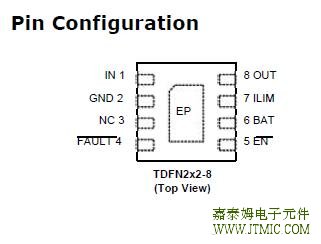
| PIN | FUNCTION | |
| NO. | NAME | |
| 1 | ||
| IN | Power Supply Input. | |
| 2 | GND | Ground. |
| 3 | NC | No Connection. |
| 4 | FAULT | Fault Indication Pin. This pin goes low when input OVP, OCP, or battery OVP is detected. |
| 5 | EN | Enable Input. Pull this pin to high to disable the device and pull this pin to low to enable device. |
| 6 | BAT | Battery OVP Sense Pin. Connect to positive terminal of battery through a resistor. |
| 7 | ILIM | Over-current Protection Setting Pin. Connect a resistor to GND to set the over-current threshold. |
| 8 | OUT | Output Voltage Pin. The output voltage follows the input voltage when no fault is detected. |
| - | EP | Exposed Thermal Pad. Must be electrically connected to the GND pin. |
六.电路原理图</span>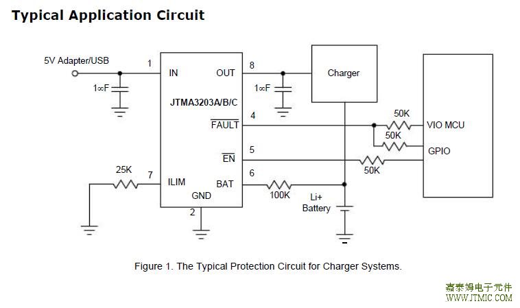
七</span>,功能概述
RBAT Selection
Connect the BAT pin to the positive terminal of battery through a resistor RBAT for battery OVP function. The RBAT
limits the current flowing from BAT to battery in case of BAT pin is shortened to VIN pin under a failure mode. The
recommended value of RBAT is 100kΩ. In the worse case of an IC failure, the current flowing from the BAT pin to the
where the 30V is the maximum IN voltage and the 3V is the minimum battery voltage. The current is so small and
can be absorbed by the charger system.
The disadvantage with the large RBAT is that the error of the battery OVP threshold will be increased. The addi-
tional error is the voltage drop across the RBAT because of the BAT bias current. When RBAT is 100kΩ, the worse-
case additional error is 100kΩx20nA=2mV, which is ac- ceptable in most applications.
REN Selection
For the same reason as the BAT pin case, the EN pin should be connected to the MCU GPIO pin through a
resistor. The value of the REN is dependent on the IO voltage of the MCU.Since the IO voltage is divided by REN and EN internal pull low resistor for EN voltage. It has to be ensured that the EN voltage is above the EN logic high voltage when the GPIO output of the MCU is high.
FAULT Output
Since the FAULT pin is an open-drain output, connecting a resistor RUP to a pull high voltage is necessary. It is also
recommended that connect the FAULT to the MCU GPIO through a resistor RFAULT. The RFAULT prevents damage to
the MCU under a failure mode. The recommended value of the resistors should be between 10kΩ to 100kΩ.
Figure 5. RUP, RFAULT, REN and RBAT
Capacitor Selection
The input capacitor is for decoupling and prevents the input voltage from overshooting to dangerous levels. In
the AC adapter hot plug-in applications or load current step-down transient, the input voltage has a transient
spike due to the parasitic inductance of the input cable. A 25V, X5R, dielectric ceramic capacitor with a value be-
tween 1 μF and 4.7 μF placed close to the IN pin is recommended.The output capacitor is for output voltage decoupling, and also can be as the input capacitor of the charging circuit.At least, a 1μF, 10V, X5R capacitor is recommended.
Layout Consideration
In some failure modes, a high voltage may be applied to the device. Make sure the clearance constraint of the PCB
layout must satisfy the design rule for high voltage.The exposed pad of the TDFN2x2-8 performs the func-
tion of channeling heat away. It is recommended that connect the exposed pad to a large copper ground plane
on the backside of the circuit board through several ther-mal vias to improve heat dissipation.The input and output capacitors should be placed close to the IC. RILIM also should be placed close to the IC.The high current traces like input trace and output trace must be wide and short.
八,相关产品
| Part_No | Package & Pins | Vin (V) | Output Current (max) (A) | Quiescent Current (typ)(uA) | Battery OVP (V) | VIN OVP | Current Limit | Power Switch On Resistance(milohm) | EN | Integrated PMOS | LDO Mode for VIN OVP | Charge Current Control | OUT Overshoot Clamp | |
| min | max | |||||||||||||
| APL3203A/B/C | TDFN2x2-8 | 4.5 | 5.5 | 1500 | 250 | 4.35 | 5.85/6.8 | Adj | 250 | Y | N | N | N | N |
| APL3203D | TDFN2x2-8 | 4.5 | 5.5 | 1500 | 250 | 4.435 | 5.85 | Adj | 250 | Y | N | N | N | N |
| APL3204A/B | TDFN4x3-12 | 4.5 | 5.5 | 1500 | 250 | 4.35 | 5.85/6.8 | Adj | 250 | Y | N | N | N | N |
| APL3205A/B | TDFN2x2-8 | 4.5 | 5.5 | 1500 | 250 | 4.35 | 5.85/6.8 | Adj | 250 | Y | N | N | N | N |
| APL3212 | TDF2x2-8 | 4.5 | 5.5 | 2000 | 250 | 4.35/4.435 | 5.85/6.8/7.2 | Adj | 130 | Y | N | N | N | N |
| APl3213/A/B | TDFN2x2-8 | 4.5 | 5.5 | 2000 | 155 | N | 5.85/5.33/5.5 | N | 80 | N | N | N | N | N |
| APl3206/A/B | TDFN2x2-8 | 4.5 | 5.5 | 700 | 250 | 4.35 | 6.17/6.8/7.65 | 1300 | 500 | N | Y | N | N | N |
| TSOT-23-6A | ||||||||||||||
| APL3208A/B/C | TDFN2x2-8 | 4.5 | 5.5 | 600 | 250 | 4.35 | 6.17 | 450/550/650 | 500 | N | Y | N | N | N |
| TSOT-23-6A | ||||||||||||||
| APL3215/A | TDFN2x2-8 | 4.5 | 5.5 | 700 | 250 | 4.35 | 6.17*6.8 | 1500 | 500 | N | Y | N | N | N |
| APL3216/A | TDFN2x2-8 | 4.5 | 9 | 700 | 250 | N | 6.8/10 | 1250 | 750 | N | Y | Y | Y | N |
| APL3218 | TDFN2x2-8 | 4.5 | 9 | 700 | 350 | N | 10 | 1200 | 750 | N | Y | Y | Y | Y |
| DFN3x3-8 | ||||||||||||||
| APL3225 | FN3x3-8 | 4.5 | 6.5 | 1000 | 350 | N | 6.8 | 1700 | 300 | |||||


发表评论