 中文
中文 English
The JTM4606 uses advanced trench technology to provide excellent RDS(ON) and low gate charge . This device is suitable for use as a load switch or in PWM applications
摘要:The JTM4606 uses advanced trench technology to provide excellent RDS(ON) and low gate charge . This device is suitable for use as a load switch or in PWM applications
目录
一,产品概述(General Description)
The JTM4606 uses advanced trench technology to provide excellent RDS(ON) and low gate charge . This device is suitable for use as a load switch or in PWM applications
二</span>.产品特点(Features)
N-Channel
VDS = 30V,ID =7.0A
RDS(ON) < 31mΩ @ VGS=10V
RDS(ON) < 43mΩ @ VGS=4.5V
P-Channel
VDS = -30V,ID = -5.1A
RDS(ON) < 95mΩ @ VGS=-4.5V
RDS(ON) < 65mΩ @ VGS=-10V
High power and current handing capability
Lead free product is acquired
Surface mount package
三</span>,应用范围 (Applications)
PWM applications
Load switch
Power management
四</span>,产品封装图 (Package)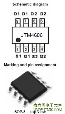
五</span>,电路原理图</span>
六</span>.产品PDF文档
 | JTM4606 |
七</span>,功能概述
| Parameter | Symbol | N-Channel | P-Channel | Unit |
| Drain-Source Voltage | VDS | 30 | -30 | V |
| Gate-Source Voltage | VGS | ±20 | ±20 | V |
| Continuous Drain Current | ID | - .1 | A | |
| Pulsed Drain Current (Note 1) | IDM | 20 | -20 | A |
| Maximum Power Dissipation | PD | 2.5 | 2.5 | W |
| Operating Junction and Storage Temperature Range | TJ,TSTG | -55 To 150 | -55 To 150 | ℃</td> |
| N+P沟道低压MOS场效应管 | |||||||||||
| 型号 | 沟道 | VDS | VGS | VTH | ID | IDM | RDS(on) | 封装 | 状态</td> | 直接替代型号 | |
| (Max) | (Max) | (Max) | |||||||||
| JTM4606 | N+P沟道 | 30V/-30V | 20V/-20V | 1.4V/ | 6.5A/ | 28A/ | 23mΩ/ | SOP8 | 量产 | AO4606/AO4603/AO4604/ | |
| -1.5V | -6A | -26A | 27mΩ | AP4503/AP4501/STM8401 | |||||||
| JTM4616 | N+P沟道 | 30V/-30V | 20V/-20V | 1.6V/ | 10.5A/ | 30A/ | 7.5mΩ/ | SOP8 | 量产 | AO4616/AO4606/AO4603/ | |
| -1.5V | -9.1A | -30A | 15mΩ | AP4604/AP4503/STM8401 | |||||||
| JTM4611 | N+P沟道 | 60V/-55V | 20V/-20V | 2.0V/ | 4.5A/ | 20A/ | 45mΩ/ | SOP8 | 量产 | AO4611/AO4612/AO4614 | |
| -2.6V | -5.0A | -25A | 64mΩ | ||||||||
| JTM6602 | N+P沟道 | 30V/-30V | 12V/-20V | 0.9V/ | 5.8A/ | 30A/ | 25mΩ/ | SOT23-6L | 量产 | AO6602/AO6604/SI3552 | |
| -1.0V | -4.2A | -30A | 50mΩ | FDC6333/FDC6327/FDC6420 | |||||||
| 备注:</td> | |||||||||||
| 1. 标注的Id电流是MOS芯片的最大常态<a href="http://www.jtm-ic.com/a/xinwenzhongxin/" target="_blank" style="padding: 0px; margin: 0px; color: rgb(37, 110, 177); text-decoration: none;">电流,实际使用时的最大常态电流还要受封装的最大电流限制。因此客户设计产品时的最大使用电流设定要考虑封装的最大电流限制。建议客户设计产品时的最大使用电流设定更重要的是要考虑MOS的内阻参数。</td> | |||||||||||
| 2. 建议在MOS的栅源(G/S)极之间并一个电阻(10K)和一个稳压二极管(5V-12V)起到保护栅源(G/S)极过压的作用。</td> | |||||||||||
| 3.建议MOS管的开启电压尽量提高,这样MOS管才能充分开启导通,这个时候内阻最小,不容易发烫。一般建议低压MOS的VGS开启电压设定为4.5V以上,中高压MOS的开启电压设定为10V以上. | |||||||||||
| 4.MOS 电路操作注意事项:</td> | |||||||||||
| 静电在很多地方都会产生,采取下面的预防措施,可以有效防止MOS 电路由于受静电放电影响而引起的损坏:</td> | |||||||||||
| • 操作人员要通过防静电腕带接地。</td> | |||||||||||
| • 设备外壳必须接地。</td> | |||||||||||
| • 装配过程中使用的工具必须接地。</td> | |||||||||||
| • 必须采用导体包装或抗静电材料包装或运输</td> | |||||||||||
| 我司的JTM2301/SOT-23/3A/20V/PMOS的<a href="http://www.jtm-ic.com/a/xinwenzhongxin/xinpinjishu/" target="_blank" style="padding: 0px; margin: 0px; color: rgb(37, 110, 177); text-decoration: none;">优点:是足3A的电流,内阻小,和<a href="http://www.jtm-ic.com/a/xinwenzhongxin/xinpinjishu/" target="_blank" style="padding: 0px; margin: 0px; color: rgb(37, 110, 177); text-decoration: none;">市场低端的1A的产品不同,可以用于移动电源/充电器/多节保护板/家电/航模/遥控玩具等大电流/低内阻的应用场合。</td> | |||||||||||
| 我司的JTM2302/SOT-23/3A/20V/NMOS的优点:是足3A的电流,内阻小,和市场低端的1A的产品不同,可以用于移动电源/充电器/多节保护板/家电/航模/遥控玩具等大电流/低内阻的应用场合。</td> | |||||||||||
| 我司的JTM3400/SOT-23-3L/5.8A/30V/NMOS的优点:是足5.8A的电流/大SOT-23封装的,内阻小,和市场低端的小SOT-23的不同,可以用于移动电源/充电器/多节保护板/家电/航模/遥控玩具等大电流/低内阻的应用场合。</td> | |||||||||||
| 我司的JTM3401/SOT-23-3L/4.2A/30V/PMOS的优点:是足4.2A的电流/大SOT-23封装的,内阻小,和市场低端的小SOT-23的不同,可以用于移动电源/充电器/多节保护板/家电/航模/遥控玩具等大电流/低内阻的应用场合。</td> | |||||||||||
| 我司的JTM2310/SOT-23-3L/3A/60V/NMOS的优点:1.耐压可达60V,足3A电流,大SOT-23封装的。2.可以用于LED照明等耐压高的产品应用。</td> | |||||||||||
| 我司的JTM4953的优点:电流大内阻小,可以用于全彩屏市场。</td> | |||||||||||
| 我司的JTM4430的优点:电流大内阻小,电流可达18A.目前市场上SOP8/NMOS电流最大的一款产品之一。</td> | |||||||||||
| 我司的JTM4440的优点:耐压可达60V, 目前市场上SOP8/NMOS耐压最大的一款产品之一。</td> | |||||||||||
| JTM8810E/SOT-26&TSSOP8/7A/20V/双NMOS的优点:足7A的电流,带ESD静电保护,相比市场上的8205,电流更大内阻更小,可直接替换AO8810/AO8820/AO8822/SSF2418E/SSF2816E,主要可用于高端的锂电保护板/手机电池/多节保护板/移动电源/充电器/家电/航模/遥控玩具等大电流/低内阻的应用场合。</td> | |||||||||||
文章标签
暂无标签


发表评论