CXSU63139是同步整流器,固定开关频率(典型为1.2兆赫),以及电流模式升压调节器。该设备允许使用USB设备的小电感和输出电容器。电流模式控制方案具有快速的瞬态响应和良好的输出电压精度,在轻负载时,CXSU63139将自动进入脉冲频率调制(PFM)操作,以降低主开关损耗
-
[ 产品资料下载 ]
目录
1.产品概述 2.产品特点
3.应用范围 4.下载产品资料PDF文档
5.产品封装图 6.电路原理图
7.功能概述 8.相关产品
一,产品概述(General Description)
The CXSU63139 is a synchronous rectifier, fixed switching frequency (1.2MHz typical), and
current-mode step-up regulator. The device allows use of small inductors and output capacitors for USB devices. The current-mode control scheme provides fast transient response and good output voltage accuracy.At light loads, the CXSU63139 will automatically enter in Pulse Frequency Modulation (PFM) operation to reduce the dominant switching losses. During PFM operation,the IC consumes very low quiescent current and maintains high efficiency over the complete load range.
The CXSU63139 also includes current-limit and over-temperature shutdown to prevent damage
in the event of an output overload.
The CXSU63139 is available in 4mmx4mm TQFN4x4-16 and DFN3x3-12 packages.
二.产品特点(Features)
1.)92% Effiicency Synchronous Boost Converter With 1000-mA Output Current From
1.8V Input
2.)Stable with Low ESR Output Capacitors
3.)Fixed 1.2MHz Oscillator Frequency
4.)Low EMI Converter (Integrated Anti-Ringing Function)
5.)Low Battery Output
6.)Integrated Power Save Mode Operation to Improve Light Load Efficiency
7.)Load Disconnected During Shutdown
8.)Output Current-Limit Protection
9.)Over Temperature Protection
10.)Under Voltage Protection
11.)Enable/Shutdown Function
12.)Available in TQFN4x4-16 and DFN3x3-12 Packages
13.)Lead Free and Green Devices Available (RoHS Compliant)
三,应用范围 (Applications)
Power Bank
Tablet
Portable Equiment
四.下载产品资料PDF文档
需要详细的PDF规格书请扫一扫微信联系我们,还可以获得免费样品以及技术支持!

五,产品封装图 (Package)

|
PIN |
NAME |
FUNCTION |
|
1,15,16 |
VOUT |
Converter Output and IC Supply Voltage. |
|
2 |
NC |
Enable in Charge Done |
|
3,4 |
SW |
Converter Switch Pin. Connect inductor here. |
|
5,6,7 |
PGND |
Enable in Charge Done |
|
8 |
VBAT |
Converter Supply Voltage. Enable in Charge Done |
|
9 |
LBI |
Low Battery Indicator. |
|
10 |
PSI |
Power Saving Input. Force VPSI exceed 1V enter PFM. Left VPSI below 0.4V enter PWM mode. |
|
11 |
EN |
Device Enable Control Input. Force VEN exceed 1V enable the device. Left VEN below 0.4V to |
|
12 |
LBO |
Low Battery Output. |
|
13 |
GND |
Signal Ground. Connect this pin to PGND. |
|
14 |
FB |
Converter Feedback Input. |
|
Exposed Pad |
PGND |
Power Ground. Tie this pin to the ground island/plane through the lowest impedance connection |
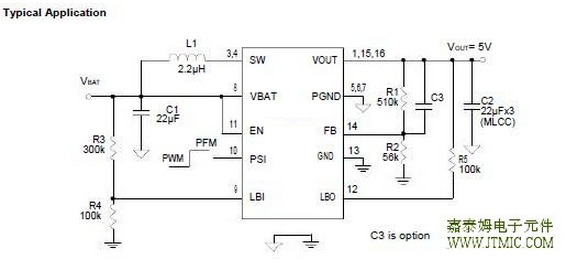
六.电路原理图
七,功能概述
Main Control Loop
The CXSU63139 is a constant frequency, synchronous rectifier, and current-mode switching regulator.
In normal operation, the internal N-channel power MOSFET is turned on each cycle when the oscillator
sets an internal RS latch and turned off when an internal comparator (ICMP) resets the latch. The peak
inductor current which ICMP resets the RS latch is controlled by the voltage on the COMP node, which
is the output of the error amplifier (EAMP). An external resistive divider connected between VOUT and
ground allows the EAMP to receive an output feedback voltage VFB at FB pin. When the load current
increases, it causes a slightly decrease in VFB relative to the 0.5V reference, which in turn causes the
COMP volt- age to increase until the average inductor current matches the new load current.
Start-up
A start-up oscillator circuit is integrated in the CXSU63139.When the device enables, the circuit pumps
the output voltage high. Once the output voltage reaches 1.6V (typ),the main DC-DC circuitry turns on
and boosts the output voltage to the final regulation voltage.
Automatic PFM/PWM mode Switch
The CXSU63139 is a fixed frequency PWM peak current modulation control step-up converter. At light
loads, theCXSU63139 will automatically enter in pulse frequency modulation operation to reduce the
dominant switching losses. In PFM operation, the inductor current may reach zero or reverse on each
pulse. A zero current comparator turns off the P-channel synchronous MOSFET, forcing DCM(Discontinuous
Current Mode) operation at light load.These controls get very low quiescent current, help to maintain
high efficiency over the complete load range.
Synchronous Rectification
The internal synchronous rectifier eliminates the need for an external Schottky diode, thus reducing cost
and board space. During the cycle off-time, the P-FET turns on and shunts the FET body diode. As a
result, the syn-chronous rectifier significantly improves efficiency with-out the addition of an external
component. Conversion efficiency can be as high as 92%.
Load Disconnect
Driving EN to ground places the CXSU63139 in shutdown mode. When in shutdown, the internal power
MOSFET turns off, all internal circuitry shuts down and the quies-cent supply current reduces to 1μA
maximum.A special circuit is applied to disconnect the load from the input during shutdown the
converter. In conventional syn-chronous rectifier circuits, the back-gate diode of the high-side P-FET
is forward biased in shutdown and allows current flowing from the battery to the output. However,this
device uses a special circuit, which takes the cath-ode of the back-gate diode of the high-side P-FET
and disconnects it from the source when the regulator is shutdown. The benefit of this feature for
the system de-sign engineer is that the battery is not depleted during shutdown of the converter.
No additional componentsmust be added to the design to make sure that the bat-tery is disconnected
from the output of the converter.
Current-Limit Protection
The CXSU63139 monitors the inductor current, flowing through the N-FET, and limits the current
peak at current-limit level to prevent loads and the CXSU63139 from dam-ages during overload
conditions.
Over-Temperature Protection (OTP)
The over-temperature circuit limits the junction tempera-ture of the CXSU63139. When the junction
temperature ex-ceeds 150oC, a thermal sensor turns off the both N-FETand P-FET, allowing the
devices to cool. The thermal sensor allows the converters to start a soft-start process and regulate
the output voltage again after the junction temperature cools by 30oC. The OTP is designed with
a 30oC hysteresis to lower the average Junction Tempera-ture (TJ) during continuous thermal overload conditions,increasing the lifetime of the device.
八,相关产品 更多同类产品......
|
Switching Regulator > Boost Converter |
|||||||||||
|
Part_No |
Package |
Archi-tecture |
Input Voltage |
Max Adj. Output Voltage |
Switch Current Limit (max) |
Fixed Output Voltage |
Switching Frequency |
Internal Power Switch |
Sync. Rectifier |
||
|
min |
max |
min |
max |
(A) |
(V) |
(kHz) |
|||||
|
SOT89 |
VM |
0.9 |
5.5 |
2.5 |
5.5 |
0.5 |
1.8|2.6|2.8|3 |3.3|3.8|4.5|5 |
- |
No |
Yes |
|
|
MSOP8|TSSOP8 |SOP8 |
VM |
2.5 |
5.5 |
2.5 |
- |
- |
- |
200 ~ 1000 |
No |
No |
|
|
TSSOP8|SOP-8P |
VM |
1 |
5.5 |
2.5 |
5 |
1 |
2.5|3.3 |
300 |
Yes |
Yes |
|
|
SOP8 |
CM |
3 |
40 |
1.25 |
40 |
1.5 |
- |
33 ~ 100 |
Yes |
No |
|
|
TQFN5x5-32 |
CM |
2.5 |
6.5 |
2.5 |
18 |
3 |
No |
1200 |
Yes |
No |
|
|
TSOT23-5 TDFN2x2-6 |
CM |
2.5 |
6 |
2.5 |
20 |
2 |
- |
1500 |
Yes |
No |
|
|
TQFN4x4-6 TDFN3x3-12 |
CM |
1.8 |
5.5 |
2.7 |
5.5 |
5 |
- |
1.2 |
Yes |
Yes |
|
|
SOT23-5 |
CM |
2.5 |
6 |
2.5 |
32 |
1 |
- |
1000 |
Yes |
No |
|
|
TSOT-23-6 TDFN2x2-8 |
CM |
1.2 |
5.5 |
1.8 |
5.5 |
1.2 |
- |
1.2 |
Yes |
Yes |
|

◀ 上一篇:2.7V至6V输入电压CXSU63138固定的开关频率1.5MHz电流模式N沟道MOSFET的升压调节器内置软启动
下一篇▶:2.5V至6V输入电压0.6ΩN沟道MOSFET内置软启动CXSU63140固定开关频率电流模式升压集成N沟道MOSFET的稳压器
| 热门信息 |
|---|
| 最新信息 |
|---|
| 推荐信息 |
|---|


