 中文
中文 English
CXSD62116A|B|C电压模式固定300kHz开关频率和同步降压控制器两个电源电压模式
|
目录 1.产品概述 2.产品特点 一,产品概述(General Description) 四.下载产品资料PDF文档 需要详细的PDF规格书请扫一扫微信联系我们,还可以获得免费样品以及技术支持! 五,产品封装图 (Package) |


|
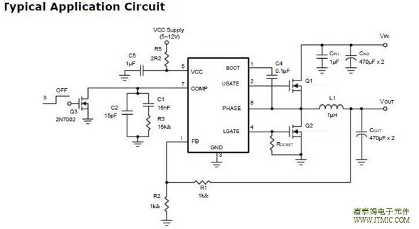
Layout Consideration (Cont.) using ground plane construction or single point grounding. Figure 8. illustrates the layout, with bold lines placed lose together. Below is a checklist for your layout: - Keep the switching nodes (UGATE, LGATE, and PHASE) away from sensitive small signal nodes since these nodes are fast moving signals. Therefore, keep traces to these nodes as short as possible. - The traces from the gate drivers to the MOSFETs (UG and LG) should be short and wide. - Place the source of the high-side MOSFET and the drain of the low-side MOSFET as close as possible. Minimiz- 八,相关产品 更多同类产品...... |

|
Switching Regulator > Buck Controller |
||||||||||
|
Part_No |
Package |
Archi tectu |
Phase |
No.of PWM Output |
Output Current (A) |
Input Voltage (V) |
Reference Voltage (V) |
Bias Voltage (V) |
Quiescent Current (uA) |
|
|
min |
max |
|||||||||
|
SOP-14 QSOP-16 QFN4x4-16 |
VM |
1 |
1 |
30 |
2.9 |
13.2 |
0.9 |
12 |
8000 |
|
|
SOP-8 |
VM |
1 |
1 |
20 |
2.9 |
13.2 |
0.8 |
12 |
5000 |
|
|
SOP-8 |
VM |
1 |
1 |
20 |
2.9 |
13.2 |
0.8 |
12 |
5000 |
|
|
QFN4x4-24 |
VM |
2 |
1 |
60 |
3.1 |
13.2 |
0.6 |
12 |
5000 |
|
|
SOP-8 |
VM |
1 |
1 |
20 |
2.2 |
13.2 |
0.8 |
5~12 |
2100 |
|
|
SOP-8 |
VM |
1 |
1 |
20 |
2.2 |
13.2 |
0.8 |
5~12 |
2100 |
|
|
SOP8|TSSOP8 |
VM |
1 |
1 |
5 |
5 |
13.2 |
1.25|0.8 |
5~12 |
3000 |
|
|
SOP-8 |
VM |
1 |
1 |
10 |
3.3 |
5.5 |
0.8 |
5 |
2100 |
|
|
SOP-14 |
VM |
1 |
1 |
10 |
5 |
13.2 |
0.8 |
12 |
2000 |
|
|
TSSOP-24 |QFN5x5-32 |
VM |
1 |
2 |
20 |
5 |
13.2 |
0.6 |
5~12 |
4000 |
|
|
SOP14 QSOP16 QFN-16 |
VM |
1 |
1 |
30 |
2.9 |
13.2 |
0.9 |
12 |
4000 |
|
|
SOP-14 |
VM |
1 |
1 |
30 |
2.2 |
13.2 |
0.6 |
12 |
5000 |
|
|
SOP-14 |
VM |
1 |
1 |
30 |
2.2 |
13.2 |
0.6 |
12 |
5000 |
|
|
SOP-14 |
VM |
1 |
1 |
25 |
2.2 |
13.2 |
0.8 |
12 |
5000 |
|
|
LQFP7x7 48 TQFN7x7-48 |
VM |
1 |
6 |
0.015 |
1.4 |
6.5 |
- |
5 |
1800 |
|
|
TSSOP-24P |
VM |
1 |
2 |
20 |
2.97 |
5.5 |
0.8 |
5~12 |
5000 |
|
|
SOP-14 |
VM |
1 |
1 |
10 |
5 |
13.2 |
0.8 |
12 |
3000 |
|
|
SOP-8-P|DIP-8 |
VM |
1 |
1 |
30 |
2.9 |
13.2 |
1.2 |
12 |
3000 |
|
|
SSOP28 QFN4x4-24 |
VM |
1 |
2 |
20 |
5 |
24 |
0.9 |
5 |
1200 |
|
|
SOP-20 |
VM |
1 |
2 |
20 |
2.2 |
13.2 |
0.6 |
5~12 |
4000 |
|


发表评论