 中文
中文 English
CXSD62106|A 同步buck-PWM控制器来产生VDDQ源极和陷极LDO线性调节器来产生VTT DDR2和DDR3内存提供完整的电源
|
目录 1.产品概述 2.产品特点 一,产品概述(General Description) voltage output in either PFM or PWM Mode. In Pulse Frequency Mode (PFM), the CXSD62106/A provides very high efficiency over light to heavy loads with loading-modulated switching frequencies. On TQFN4x4- 24A package, the Forced PWM Mode works nearly at con-stant frequency for low-noise requirements. and output over-voltage protections.A Power-On-Reset function monitors the voltage on VCC prevents wrong operation during power on.The LDO is designed to provide a regulated voltage with bi-directional output current for DDR-SDRAM termination.The device integrates two power transistors to source or sink current up to 1.5A. It also incorporates current-limit and thermal shutdown protection. The output voltage of LDO tracks the voltage at VTTREF pin. An internal resistor divider is used to provide a half voltage of VDDQ for VTTREF and VTT Voltage. The VTT output voltage is only requiring 20μF of ceramic output capacitance for stability and fast transient response. The S3 and S5 pins provide the sleep state for VTT (S3 state)and suspend state (S4/S5 state) for device, when S5 and CXSD62106A is available in 3mmx3mm 20-pin TQFN package. Independent Over-Current-Limit (OCL) Thermal Shutdown Protection QFN-24 4mmx4mm Thin Package (TQFN4x4-24A) |
三,应用范围 (Applications)
DDR2, and DDR3 Memory Power Supplies
SSTL-2 SSTL-18 and HSTL Termination
四.下载产品资料PDF文档
需要详细的PDF规格书请扫一扫微信联系我们,还可以获得免费样品以及技术支持!

五,产品封装图 (Package)


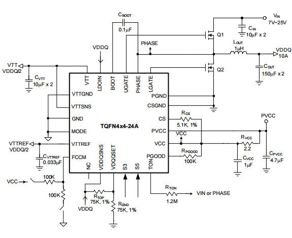
六.电路原理图

七,功能概述
Layout Consideration (Cont.)
· Keep the switching nodes (UGATE, LGATE, BOOT, and PHASE) away from sensitive small signal nodes
(VDDQSET, VTTREF, CS, and MODE) since these nodes are fast mov ing signals. Therefore, keep traces
to these nodes as short as possible and there should be no other weak signal traces in parallel with theses
traces on any layer.
The signals going through theses traces have both high dv/dt and high di/dt, with high peak charging and
discharging current. The traces from the gate drivers to the MOSFETs (UGATE and LGATE) should be short
and wide.
Place the source of the high-side MOSFET and the drain of the low-side MOSFET as close as possible. Mini-
mizing the impedance with wide layout plane between the two pads reduces the voltage bounce of the node.
ceramic capacitor near the drain of the high-side MOSFET as close as possible. The bulk capacitors are
also placednear the drain).
The input capacitor should be near the drain of the up per MOSFET; the high quality ceramic decoupling ca-
pacitor can be put close to the VCC and GND pins; the VTTREF decoupling capasitor should be close to the
VTTREF pin and GND; the VDDQ and VTT output ca-pacitors should be located right across their output pin
as clase as possible to the part to minimize parasitics.
The input capacitor GND should be close to the output capacitor GND and the lower MOSFET GND.
· The drain of the MOSFETs (VIN and PHASE nodes) should be a large plane for heat sinking. And PHASE
pin traces are also the return path for UGATE. Connect this pin to the converter’s upper MOSFET source.
· The CXSD62106/A used ripple mode control. Build the resistor divider close to the VDDQSET pin so that the
high imped ance trace is shorter when the output volt-age is in ad justable mode. And the VDDQSET pin
traces can’t be closed to the switching signal traces (UGATE, LGATE, BOOT, and PHASE)
The PGND trace should be a separate trace, and inde pendently go to the source of the low-side MOSFETs
for current limit accuracy.Decoupling capacitor, the resistor dividers, boot capacitors, and current limit stetting resistor should be close their pins. (For example, place the decoupling
八,相关产品 更多同类产品......
|
Switching Regulator > Buck Controller |
||||||||||
|
Part_No |
Package |
Archi tectu |
Phase |
No.of PWM Output |
Output Current (A) |
Input Voltage (V) |
Reference Voltage (V) |
Bias Voltage (V) |
Quiescent Current (uA) |
|
|
min |
max |
|||||||||
|
SOP-14 QSOP-16 QFN4x4-16 |
VM |
1 |
1 |
30 |
2.9 |
13.2 |
0.9 |
12 |
8000 |
|
|
SOP-8 |
VM |
1 |
1 |
20 |
2.9 |
13.2 |
0.8 |
12 |
5000 |
|
|
SOP-8 |
VM |
1 |
1 |
20 |
2.9 |
13.2 |
0.8 |
12 |
5000 |
|
|
QFN4x4-24 |
VM |
2 |
1 |
60 |
3.1 |
13.2 |
0.6 |
12 |
5000 |
|
|
SOP-8 |
VM |
1 |
1 |
20 |
2.2 |
13.2 |
0.8 |
5~12 |
2100 |
|
|
SOP-8 |
VM |
1 |
1 |
20 |
2.2 |
13.2 |
0.8 |
5~12 |
2100 |
|
|
SOP8|TSSOP8 |
VM |
1 |
1 |
5 |
5 |
13.2 |
1.25|0.8 |
5~12 |
3000 |
|
|
SOP-8 |
VM |
1 |
1 |
10 |
3.3 |
5.5 |
0.8 |
5 |
2100 |
|
|
SOP-14 |
VM |
1 |
1 |
10 |
5 |
13.2 |
0.8 |
12 |
2000 |
|
|
TSSOP-24 |QFN5x5-32 |
VM |
1 |
2 |
20 |
5 |
13.2 |
0.6 |
5~12 |
4000 |
|
|
SOP14 QSOP16 QFN-16 |
VM |
1 |
1 |
30 |
2.9 |
13.2 |
0.9 |
12 |
4000 |
|
|
SOP-14 |
VM |
1 |
1 |
30 |
2.2 |
13.2 |
0.6 |
12 |
5000 |
|
|
SOP-14 |
VM |
1 |
1 |
30 |
2.2 |
13.2 |
0.6 |
12 |
5000 |
|
|
SOP-14 |
VM |
1 |
1 |
25 |
2.2 |
13.2 |
0.8 |
12 |
5000 |
|
|
LQFP7x7 48 TQFN7x7-48 |
VM |
1 |
6 |
0.015 |
1.4 |
6.5 |
- |
5 |
1800 |
|
|
TSSOP-24P |
VM |
1 |
2 |
20 |
2.97 |
5.5 |
0.8 |
5~12 |
5000 |
|
|
SOP-14 |
VM |
1 |
1 |
10 |
5 |
13.2 |
0.8 |
12 |
3000 |
|
|
SOP-8-P|DIP-8 |
VM |
1 |
1 |
30 |
2.9 |
13.2 |
1.2 |
12 |
3000 |
|
|
SSOP28 QFN4x4-24 |
||||||||||


发表评论