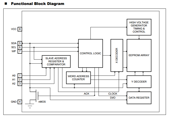
CX24C512 CX24C512G是使用工业标准2线接口进行通信的EEPROM设备。CX24C512G包含一个512K位(65536x8)的内存数组,该数组按每页128字节进行组织。EEPROM可以在1.7V到5.5V的宽电压范围内工作,适合大多数应用。本产品可提供低功耗2线EEPROM解决方案。该设备提供无铅、RoHS、无卤素或绿色。可用的封装类型有8针SOIC/SOP、TSSOP、DFN和CSP。CX24C512Gis与工业标准2线总线协议兼容。如果总线没有响应,新发送的操作码命令将重置总线,设备将正确响应。简单总线由串行时钟线(SCL)和串行数据线(SDA)组成。利用这种总线协议,主设备,例如微控制器,通常可以控制一个或多个从设备,类似于CX24C512G,SDA线路上的位流包括一系列字节,这些字节标识特定的从设备、指令、该从设备内的地址和一系列数据(如果合适)。CX24C512Galso有一个写保护管脚(WP),允许阻塞指定内存区域上的任何写操作。在任何情况下,设备都不会被挂断。为了防止状态机在通电顺序期间进入错误状态或在条件下关闭电源开关
内置上电复位电路。在通电过程中,直到电源电压(VCC)达到高于重置阈值电压的可接受稳定水平,设备才会响应任何指令。一旦VCC通过上电重置阈值,设备将重置并进入待机模式。这还可以避免在通电阶段执行任何意外的写入操作。在断电过程中,一旦VCC降至开机复位阈值电压以下,设备将进入待机模式。此外,在没有内部写操作进行的情况下,设备在接收到停止命令后将处于待机模式。然而,除非VCC在其操作级别内,否则发送命令是非法的。两线串行接口,I2C TM兼容
–双向数据传输协议
宽电压运行——VCC=1.7V至5.5V
速度:400 KHz(1.7V)和1 MHz(2.5V~5.5V)
备用电流(最大值):1
μA,1.7V工作电流(最大值):2毫安,1.7V
硬件数据保护-写保护引脚
顺序和随机读取特性
存储组织:65536 x 8位
页面大小:128字节
页面写入模式
–每页最多可写入128字节
自动清除的自动定时写入周期:5ms(最大值)
过滤输入以抑制噪声
高可靠性
–耐久性:100万次循环
–数据保留:100年
工业温度等级
包装:SOIC/SOP、TSSOP、DFN和CSP
无铅、RoHS、无卤、绿色
-
[ CX24C512 ]
目录
产品概述 返回TOP
TheCX24C512 CX24C512G are EEPROM devices that use the industrial standard 2-wire interface for communications. The CX24C512 CX24C512G contains a memory array of 512K-bits (65,536x8), which is organized in 128-byte per page. The EEPROM can operate in a wide voltage range from 1.7V to 5.5V which fits most application. This product can provide a low-power 2-wire EEPROM solution. The device is offered in Lead-free, RoHS, halogen free or Green. The available package types are 8-pin SOIC/SOP, TSSOP, DFN and CSP. The CX24C512 CX24C512Gis compatible with the industrial standard 2-wire bus protocol. If in case the bus is not responded, a new sent Op-code command will reset the bus and the device will respond correctly. The simple bus consists of the Serial Clock wire (SCL) and the Serial Data wire (SDA). Utilizing such bus protocol, a Master device, such as a microcontroller, can usually control one or more Slave devices, alike this CX24C512G The bit stream over the SDA line includes a series of bytes, which identifies a particular Slave device, an instruction, an address within that Slave device, and a series of data, if appropriate. The CX24C512Galso has a Write Protect pin (WP) to allow blocking any write operations over specified memory area. Under no circumstance, the device will be hung up. In order to refrain the state machine entering into a wrong state during power-up sequence or a power toggle off-on condition, a power on reset circuit is embedded. During power-up, the device does not respond to any instructions until the supply voltage (VCC) has reached an acceptable stable level above the reset threshold voltage. Once VCC passes the power on reset threshold, the device is reset and enters into the Standby mode. This would also avoid any inadvertent Write operations during power-up stage. During power-down process, the device will enter into standby mode, once VCC drops below the power on reset threshold voltage. In addition, the device will be in standby mode after receiving the Stop command, provided that no internal write operation is in progress. Nevertheless, it is illegal to send a command unless the VCC is within its operating level.
产品特点 返回TOP
Two-Wire Serial Interface, I2C TM Compatible
– Bi-directional data transfer protocol
Wide-voltage Operation – VCC = 1.7V to 5.5V
Speed: 400 KHz (1.7V) and 1 MHz (2.5V~5.5V)
Standby current (max.): 1A, 1.7V
Operating current (max.): 2 mA, 1.7V
Hardware Data Protection – Write Protect Pin
Sequential & Random Read Features
Memory organization: 65,536 x 8 bits
Page Size: 128 bytes
Page write mode
– Up to 128 bytes per page write
Self timed write cycle with auto clear: 5ms (max.)
Filtered inputs for noise suppression
High-reliability
– Endurance: 1 million cycles
– Data retention: 100 years
Industrial temperature grades
Packages: SOIC/SOP, TSSOP, DFN and CSP
Lead-free, RoHS, Halogen free, Green
应用范围 返回TOP
a
技术规格书(产品PDF) 返回TOP
需要详细的PDF规格书请扫一扫微信联系我们,还可以获得免费样品以及技术支持!

产品封装图 返回TOP

电路原理图 返回TOP
相关芯片选择指南 返回TOP
| 串行存储器 (Serial EEPROM ) | ||||
| Part No. | Capacity | Interface | VDD | Package |
| CX24C02 | 2K bits | Two-wire Serial | 1.7~5.5V | DIP8 SOP8 TSSOP8 DFN8 |
| CX24C04 | 4K bits | Two-wire Serial | 1.7~5.5V | DIP8 SOP8 TSSOP8 DFN8 |
| CX24C08 | 8K bits | Two-wire Serial | 1.7~5.5V | DIP8 SOP8 TSSOP8 DFN8 |
| CX24C16 | 16K bits | Two-wire Serial | 1.7~5.5V | DIP8 SOP8 TSSOP8 DFN8 |
| CX24C32A | 32K bits | Two-wire Serial | 1.7~5.5V | DIP8 SOP8 TSSOP8 UDFN8 WCSP4 |
| CX24C32B | 32K bits | Two-wire Serial | 1.7~5.5V | DIP8 SOP8 TSSOP8 UDFN8 WCSP4 |
| CX24C64A | 64K bits | Two-wire Serial | 1.7~5.5V | DIP8 SOP8 TSSOP8 UDFN8 WCSP4 |
| CX24C64B | 64K bits | Two-wire Serial | 1.7~5.5V | DIP8 SOP8 TSSOP8 UDFN8 WCSP4 |
| CX24C128A | 128K bits | Two-wire Serial | 1.7~5.5V | DIP8 SOP8 TSSOP8 UDFN8 WCSP4 |
| CX24C128B | 128K bits | Two-wire Serial | 1.7~5.5V | DIP8 SOP8 TSSOP8 UDFN8 WCSP4 |
| CX24C256 | 256K bits | Two-wire Serial | 1.7~5.5V | DIP8 SOP8 TSSOP8 |
| CX24C512 | 512K bits | Two-wire Serial | 1.7~5.5V | SOP8 TSSOP8 DFN8 |
| CX24C512G | 513K bits | Two-wire Serial | 1.7~5.6V | SOP8 TSSOP8 DFN9 |
◀ 上一篇:CX24C256提供262144位串行电可擦可编程只读存储器EEPROM每8位32768字存储敏感的应用程序参数I2C双向数据传输协议施密特触发器噪声抑制的滤波输入
下一篇▶:CX24C512G
| 热门信息 |
|---|
| 最新信息 |
|---|
| 推荐信息 |
|---|


