 中文
中文 English
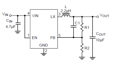
CXSD61044D high-efficiency, high frequency synchronous step-down DC-DC regulator ICs capable of delivering up to 1.5A output currents
| 产品型号: | CXSD61044D |
| 产品类型: | DC-DC转换器 |
| 产品系列: | 同步DC-DC降压IC |
| 产品状态: | 量产 |
| 浏览次数: | 89 次 |
产品简介
from 2.3V to 6.0V and integrate main switch and synchronous switch
with very low RDS(ON) to minimize the conduction loss
技术参数
| 输入电压范围 (VIN) | - 2.3V-6.5V |
|---|---|
| 输出电压 (VOUT) | 可调输出 |
| 输出电流 (IOUT) | 1.3A |
| 工作频率 | 1.5M |
| 转换效率 | 96% |
| 封装类型 | DFN2*2-6 |
| Topology | 低压同步DC降压 |
| Control method | PWM/PFM |
| Switching frequency | 1.5M |
| Protection | Auto-recovery |
| Features | 静态工作电流IQ(typ):35uA |
| Operating temp | -40℃~125℃ |
| Reference design | 反馈电压:0.6V |
| Precision | ±2.5% |
| 待机电流 | 35uA |
产品详细介绍
目录
1.产品概述 2.产品特点
3.应用范围 4.下载产品资料PDF文档
5.产品封装图 6.电路原理图
7.功能概述 8.相关产品
一,产品概述(General Description)
The CXSD61039 CXSD61044D are high-efficiency, high frequency synchronous
step-down DC-DC regulator ICs capable of delivering up to 1.5A output
currents. The CXSD61039 can operate over a wide inpu tvoltage range
from 2.3V to 6.0V and integrate main switch and synchronous switch
with very low RDS(ON) to minimize the conduction loss.
It is ideal for powering portable equipment that runs from a single cell
Lithium-Ion (Li+) battery. The CXSD61039 output voltage can be regulated
as low as 0.6V. The CXSD61039 CXSD61044D can also run at 100% duty cycle for low dropout operation, extending battery life in portable system. This device offers
two operation modes,PWM control and PFM Mode switching control,which
allows a high efficiency over the wider range of the load.
The CXSD61039 CXSD61044D is off ered in a low profile (1mm)5-pin, thin SOT package, and is available in an adjustable version.
二.产品特点(Features)
High Efficiency: Up to 96%
1.0MHz Constant Frequency Operation
2A Output Current
No Schottky Diode Required
2.3V to 6V Input Voltage Range
Output Voltage as Low as 0.6V
PFM Mode for High Efficiency in Light Load
100% Duty Cycle in Dropout Operation
Low Quiescent Current: 40μA
Short Circuit Protection
Thermal Fault Protection
Inrush Current Limit and Soft Start
Input overvoltage protection(OVP)
<1μA Shutdown Current
SOT23-5 package
三,应用范围 (Applications)
Cellular and Smart Phones
Wireless and DSL Modems
PDAs
Portable Instruments
Digital Still and Video Cameras
PC Cards
四.技术规格书下载(产品PDF)
需要详细的PDF规格书请扫一扫微信联系我们,还可以获得免费样品以及技术支持!

五,产品封装图 (Package)


|
PIN |
NAME |
FUNCTION |
|
1 |
RUN |
Chip Enable Pin. Drive RUN above 1.5V to turn on the part. Drive |
|
2 |
GND |
Ground Pin |
|
3 |
SW |
Power Switch Output. It is the switch node connection to Inductor. |
|
4 |
VIN |
Power Supply Input. Must be closely decoupled to GND with a 10μF or greater ceramic capacitor. |
|
5 |
VOUT |
Output Voltage Feedback Pin. An internal resistive divider divides the output voltage down for comparison to the internal reference voltage. |
六.电路原理图

七,功能概述
|
Parameter |
Conditions |
MIN |
TYP |
MAX |
unit |
|
Input Voltage Range |
2.3 |
6.0 |
V |
||
|
UVLO Threshold |
1.7 |
1.9 |
2.1 |
V |
|
|
Input DC Supply Current |
(Note 4) |
140 |
300 |
μA |
|
|
Regulated Feedback Voltage |
TA = 25°C |
0.588 |
0.600 |
0.612 |
V |
|
TA = 0°C ≤ TA ≤ 85°C |
0.586 |
0.600 |
0.613 |
V |
|
|
TA = -40°C ≤ TA ≤ 85°C |
0.585 |
0.600 |
0.615 |
V |
|
|
Reference Voltage Line |
Vin=2.3V to 6.0V |
0.04 |
0.40 |
%/V |
|
|
Output Voltage Line |
VIN = 2.3V to 6.0V |
0.04 |
0.4 |
% |
|
|
Output Voltage Load |
0.5 |
% |
|||
|
Oscillation Frequency |
Vout=100% |
1.0 |
MHz |
||
|
300 |
KHz |
||||
|
On Resistance of PMOS |
ISW=100mA |
0.2 |
Ω |
||
|
ON Resistance of NMOS |
ISW=-100mA |
0.13 |
Ω |
||
|
Peak Current Limit |
VIN= 3V, Vout=90% 3410A |
2.5 |
A |
||
|
VIN= 3V, Vout=90% 3410 |
2.5 |
A |
|||
|
RUN Threshold |
0.30 |
1.0 |
1.50 |
V |
|
|
RUN Leakage Current |
±0.01 |
±1.0 |
μA |
||
|
SW Leakage Current |
VRUN=0V,VIN=Vsw=5V |
±0.01 |
±1.0 |
μA |
八,相关芯片选择指南 更多同类产品......
|
低压同步DC-DC降压IC |
|||||||||
|
型号 |
输入耐压 |
输出电压 |
输出电流 |
反馈电压 |
工作频率 |
效率 |
静态工作电流 |
待机电流 |
封装 |
|
2.0-6.0V |
1.2V/1.8V/3.3V/可调输出 |
0.7A |
0.6V |
1.5MHz |
96% |
20uA |
SOT-25 |
||
|
2.5-6.0V |
可调输出 |
1A |
0.6V |
1.5MHz |
96% |
20uA |
SOT-25 |
||
|
2.0-6.0V |
可调输出 |
1.0A |
0.6V |
1.5M |
96% |
20uA |
1uA |
SOT-25 |
|
|
2.3-6.0V |
可调输出 |
1.2A |
0.6V |
1.5M |
96% |
35uA |
1uA |
SOT-25 |
|
|
2.3-6.0V |
可调输出 |
1.5A |
0.6V |
1.5M |
96% |
35uA |
1uA |
SOT-25 |
|
|
2.3-6.0V |
可调输出 |
1.5A |
0.6V |
1.5M |
96% |
35uA |
1uA |
SOT-25 |
|
|
2.0-6.5V |
可调输出 |
2.0A |
0.6V |
1.5M |
96% |
40uA |
1uA |
SOT-26 |
|
|
2.6-6.0V |
可调输出 |
2.0A |
0.6V |
3M |
96% |
30uA |
0.1uA |
SOT-25 |
|
|
2.3-6.5V |
可调输出 |
2.0A |
0.6V |
1.5M |
96% |
40uA |
40uA |
SOP-8 |
|
|
2.3-6.5V |
可调输出 |
3.0A |
0.6V |
1.5M |
95% |
40uA |
40uA |
ESOP-8 |
|
|
2.3V-6.5V |
可调输出 |
1.3A |
0.6V |
1.5M |
96% |
35uA |
35uA |
DFN2*2-6 |
|
|
2.3V-6.5V |
可调输出 |
2A |
0.6V |
1.5M |
95% |
40uA |
40uA |
DFN3*3-10 |
|
|
2.5-6.0V |
可调输出 |
3.0A |
0.6V |
1MHz |
95% |
40uA |
0.1uA |
SOT-25 |
|

用户评论