 中文
中文 English
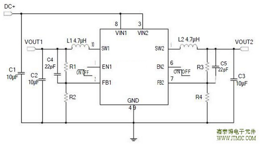
2.5V到5.5V的输入电压DC/DC转换器高效的同步双通道脉冲宽度调制降压型CXSD6109 PWM/PFM模式切换700mA负载电流
| 产品型号: | CXSD6109 |
| 产品类型: | DC-DC转换器 |
| 产品系列: | Buck降压型芯片 |
| 产品状态: | 量产 |
| 浏览次数: | 86 次 |
产品简介
转换器具有独立的使能输入和短路保护多功能功率序列组合。
技术参数
| 输入电压范围 (VIN) | 2.5 ~ 5.5V |
|---|---|
| 输出电压 (VOUT) | 0.6V ~ 5.5V |
| 输出电流 (IOUT) | 700mA |
| 工作频率 | 1.4MHz |
| 转换效率 | 95% |
| 封装类型 | DFN3*3-10L |
| Topology | Buck降压型芯片 |
| Control method | PWM/PFM |
| Switching frequency | 1.4MHz |
| Protection | 过流/过压/过温 |
| Operating temp | -40℃~125℃ |
产品详细介绍
目录
1.产品概述 2.产品特点
3.应用范围 4.下载产品资料PDF文档
5.产品封装图 6.电路原理图
7.功能概述 8.相关产品
一,产品概述(General Description) ![]()
The CXSD6109 is a high efficiency synchronous,dual channel PWM step-down
DC/DC converter working under an input voltage range from 2.5V to 5.5V. It
integrates two PWM synchronous step-down DC-DC converters. 100% duty cycle
capability extends battery life in portable devices,while the quiescent current (one
channel) is 200μA with no load, and drops to<1μA in shutdown.Each DC-DC
converter has independent enable input and short-circuit protection allowing
versatile power sequence combination. The CXSD6109 converters are available
in the industry standard DFN3*3-10L packages (or upon request).
二.产品特点(Features)![]()
Up to 94% Efficiency
Current Mode Operation for Excellent Line
and Load Transient Response
Up to 700mA Load Current
Low Quiescent Current (one Channel) :200μA
Output Voltage: 0.6V ~ 5.5V
Automatic PWM/PFM Mode Switching
No Schottky Diode Required
1.4MHz Constant Frequency Operation
Short-Circuit Protection
Shutdown Quiescent Current: < 1μA
DFN3*3-10L Package
三,应用范围 (Applications)![]()
Digital cameras and MP3
Palmtop computers / PDAs
Cellular phones
Wireless handsets and DSL modems
PC cards
四.技术规格书下载(产品PDF)
需要详细的PDF规格书请扫一扫微信联系我们,还可以获得免费样品以及技术支持!

五,产品封装图 (Package)![]()

六.电路原理图![]()
七,功能概述![]()
Power Dissipation………………………………………………………………………Internally limited
Supply Input Voltage,VIN1,VIN2………………………………………………..………..…..-0.3V ~ 6V
Output Voltage, VOUT1,VOUT2……………………………………………….....……….....-0.3V ~ 6V
EN1, EN2 Pin Voltage………………………………..………………………...……-0.3V ~ (VIN+0.3)V
SW1, SW2 Pin Voltage……………………………………………………….………-0.3V ~ (VIN+0.3)V
SW1,SW2 Pin Current….……………………………………………………………………………..1.3A
Operating Temperature Range(Note 2) ………………………………………………...-40℃ ~ + 85℃
Storage Temperature Range ………………………………………………….……….-65℃ ~ + 150℃
Junction Temperature ……………………………………………………………...……-40℃ ~ +125℃
Lead Temperature (Soldering 10 sec.) ……………………………………………….…………..+ 265℃
八,相关芯片选择指南 更多同类产品......![]()
|
DC-DC降压 |
|||||
|
Model |
VIN (V) |
VOUT (V) |
ISW |
FOSC(MHz) |
Package |
|
0.6V ~5V |
0.6 ~ 5.5 |
1.3A |
1~1.4 |
SOT-23-5L |
|
|
5V~16V |
1.2V~16V |
2A |
400kHz |
SOP-8L |
|
|
2.5 ~ 5.5 |
0.6 ~ 5.5 |
1.3A |
1~1.4 |
SOT-23-5L |
|
|
2.5 ~ 5.5 |
0.6V ~ 5.5V |
700mA |
1.4MHz |
DFN3*3-10L |
|
|
2.5V ~5.5V |
0.6V ~ 5.5V |
3A |
950kHz |
SOT-23-5L |
|
|
2.5V ~5.5V |
0.6V ~ 5.5V |
1.4A |
950kHz |
SOT-23-5L |
|
|
10V ~ 30V |
0.6V ~ 5.5V |
2.5A |
500k |
SOP-8 |
|
|
8V ~ 30V |
0.6V ~ 5.5V |
3.5A |
500KHz |
SOP8 |
|
|
8V ~ 30V |
0.6V ~ 5.5V |
3.0A |
500KHz |
SOP8 |
|
|
8V ~ 30V |
0.6V ~ 5.5V |
2A |
500KHz |
SOP8 |
|

用户评论