 中文
中文 English
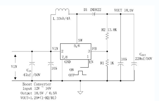
N沟道功率MOSFET固定频率振荡器3.6V至24V输入电压CXSU6310正负输出电压单反馈引脚编程电流模式控制
| 产品型号: | CXSU6310 |
| 产品类型: | DC-DC转换器 |
| 产品系列: | 同步DC-DC升压IC |
| 产品状态: | 量产 |
| 浏览次数: | 93 次 |
产品简介
技术参数
| 输入电压范围 (VIN) | - 3.6V ~ 24V |
|---|---|
| 输出电压 (VOUT) | 60V |
| 输出电流 (IOUT) | 2A |
| 工作频率 | 400KHz |
| 转换效率 | 90% |
| 封装类型 | SOP8L |
| Features | 背光驱动 |
| Topology | 白灯背光驱动IC |
| Efficiency | .94 |
| Protection | 过压过流保护 |
| 调光形式 | 背光驱动, 白灯背光驱动IC, , .94, 过压过流保护, , 100Hz-1KHz, , 背光驱动 |
| Pwm frequency | 100Hz-1KHz |
| Application type | 背光驱动 |
产品详细介绍
目录
1.产品概述 2.产品特点 3.应用范围 4.技术规格书下载(产品PDF文档)
5.产品封装图 6.电路原理图 7.功能概述 8.相关产品
一,产品概述(General Description) ![]()
The CXSU6310 regulator is a wide input range,current mode,
DC/DC converter which is capable of generating either positive or
negative output voltages. It can be configured as either a boost,
flyback, SEPIC or inverting converter. The CXSU6310 built in
N-channel power MOSFET and fixed frequency oscillator,
current-mode architecture results in stable operation over a
wide range of supply and output voltages.
The CXSU6310 regulator is special design for portable
electronic equipment.
二.产品特点(Features)![]()
Wide 3.6V to 24V Input Voltage Range
Positive or Negative Output Voltage
Programming with a Single Feedback Pin
Current Mode Control Provides Excellent
Transient Response
1.25V reference adjustable version
Fixed 400KHz Switching Frequency
Maximum 2A Switching Current
SW PIN Built in Over Voltage Protection
Excellent line and load regulation
EN PIN TTL shutdown capability
Internal Optimize Power MOSFET
High efficiency up to 90%
Built in Frequency Compensation
Built in Soft-Start Function
Built in Thermal Shutdown Function
Built in Current Limit Function
Available in SOP8L package
三,应用范围 (Applications)![]()
Automotive and Industrial Boost
Buck-Boost / Inverting Converters
Portable Electronic Equipment
四.技术规格书下载(产品PDF)![]()
需要详细的PDF规格书请扫一扫微信联系我们,还可以获得免费样品以及技术支持!

五,产品封装图 (Package)![]()

|
Pin Number |
Pin Name |
Description |
|
1 |
EN |
Enable Pin. Drive EN pin low to turn off the device, drive it |
|
2 |
VIN |
Supply Voltage Input Pin. CXSU6310 operates from a 3.6V to 24V DC voltage. Bypass Vin to GND with a suitably large capacitor |
|
3 |
FB |
Feedback Pin (FB). The feedback threshold voltage is 1.25V. |
|
4 |
NC |
No Connected. |
|
5,6 |
SW |
Power Switch Output Pin (SW). Output is the switch node that |
|
7,8 |
GND |
Ground Pin. |
六.电路原理图![]()
七,功能概述![]()
|
Parameter |
Symbol |
Value |
Unit |
|
Input Voltage |
Vin |
-0.3 to 26 |
V |
|
Feedback Pin Voltage |
VFB |
-0.3 to Vin |
V |
|
EN Pin Voltage |
VEN |
-0.3 to Vin |
V |
|
Output Switch Pin Voltage |
VOutput |
-0.3 to 60 |
V |
|
Power Dissipation |
PD |
Internally limited |
mW |
|
Thermal Resistance (SOP-8L) |
RJA |
100 |
oC/W |
|
Operating Junction Temperature |
TJ |
-40 to 125 |
oC |
|
Storage Temperature |
TSTG |
-65 to 150 |
oC |
|
Lead Temperature (Soldering, 10 sec) |
TLEAD |
260 |
oC |
|
ESD (HBM) |
>2000 |
V |
八,相关芯片选择指南![]()
|
升压型直流电源变换器芯片 |
||||||
|
产品型号 |
输入电压 |
最大输出电压 |
开关电流 |
开关频率 |
电压版本 |
封装形式 |
|
3.6V ~ 24V |
60V |
2A |
400KHz |
Adj (1.25V) |
SOP8L |
|
|
3.6V ~ 32V |
60V |
3A |
400KHz |
Adj (1.25V) |
TO252-5L |
|
|
5V ~ 40V |
60V |
5A |
180KHz |
Adj (1.25V) |
TO263-5L |
|
|
5V ~ 40V |
60V |
5A |
180KHz |
Adj (1.25V) |
TO220-5L |
|

用户评论