

目录
一,产品概述(General Description)
The KT0913 is a fully integrated digital AM/FM radio receiver chip with patented technologies that offer full band AM/FM functionality, high quality audio performance, simple design and low BOM cost thanks to the minimum external components required and direct frequency and volume control interface without requiring customers to modify existing exterior module.
Thanks to the patented tuning technology, the receiver maintains good signal reception even with short antennas. The chip consumes merely 22mA current and can be powered by 2 AAA batteries. Another useful feature is that the volume and channel information can be preserved in standby mode without external memories. KT0913 supports a wide range of reference clocks from 32.768KHz to 26MHz, hence can share system clocks with a varieties of MCUs further reducing the system BOM cost.With high audio performance, fully integrated features and
low BOM cost, KT0913 is ideal for various applications and products.
二.产品特点(Features)
Worldwide full band FM/AM support
FM: 32MHz-110MHz
AM: 500KHz-1710KHz
Fully integrated frequency synthesizer with no external component
High Sensitivity
1.6uVEMF for FM
16uVEMF for AM
High Fidelity
SNR (FM/AM): 60dB/55dB
THD: 0.3%
Low Supply Current
22mA (operating)
<15uA (standby)
Advanced features
Automatic antenna tuning
Adjustable AM channel filters (2/4/6KHz)
Automatic Frequency Control (AFC)
Automatic Gain Control (AGC)
Embedded FM SNR meter
Fast seek/Tune
Integrated stereo headphone driver
I2C control interface for MCU
Special Features:
Support traditional dial and digital key for
frequency tuning and volume control
Memorize channel and volume in standby mode
Low supply voltage: 2.1V to 3.6V, can be supplied by 2
AAA batteries
Support both 32.768KHz and 38KHz crystal
Support continuous reference frequency from 32.768KHz
to 26MHz
Small form factor SSOP16L package
RoHS Compliant
三,应用范围 (Applications)
Desktop and portable radio, mini/portable audio systems,
clock radio, campus radio, PMP docking station, car audio
system, toy and gift
四,产品封装图 (Package)

五,电路原理图

六, 产品PCB
PCB 版图有什么需要注意的?
1)电源的去藕电容应该尽量靠近电源输入脚,并保证流入芯片的电流都先经过电容滤波。
2)不要将 RF 走线、数字走线、模拟走线平行放置,避免它们之间信号耦合,减少干扰。
3)不要将 RF 输入线打断,或是穿过两层走线。
4)RF 输入端的走线要尽量的短,最好将 RF input 安排在 PCB 的板边处。
5)RF 输入脚及走线周围需要使用铺地将其包裹起来,避免受到其他信号的干扰,但是注意不
要将地线与 RF 信号靠的太近,避免过大的分布电容衰减 RF 信号。2)不要将 RF 走线、数字走线、模拟走线平行放置,避免它们之间信号耦合,减少干扰。
3)不要将 RF 输入线打断,或是穿过两层走线。
4)RF 输入端的走线要尽量的短,最好将 RF input 安排在 PCB 的板边处。
5)RF 输入脚及走线周围需要使用铺地将其包裹起来,避免受到其他信号的干扰,但是注意不
6) I2C 接口走线不要横穿芯片,尽量不跨层。如有可能,在 I2C 走线的背面并排保持地线或地
平面,直至主控芯片的地平面,以此降低 I2C 接口对芯片的干扰。
7) 确保 DVSS、AVSS、RFGND 可以很好的共地,不要在芯片下面走线。
七.产品BOM
| 器件 | 描述/数值 |
| C1 | 0.1uF 去耦电容 |
| C2,C3 | 24pF 谐振电容 |
| L1 | AM 天线,350uH |
| E1 | FM 天线 |
| Y1 | 32.768kHz 晶体 |
| SW1 | 开关 |
| R1,R2 | 10Kohm 保护电阻 |
| R3,R4 | 可调电阻 |
| K1,K2,K3,K4 | 按键 |
 |
kt0913 |
九,功能概述
KT0913 可以支持 MCU 通过 I2C 总线、改变变阻器的数值、按键这三种方式来控制芯片的音量
和接收频率。
当使用变阻器方式时需要通过 I2C 总线将寄存器 0x1D 的 bit3:2 和 bit1:0 配置都为 b’10。
当使用按键方式时需要通过 I2C 总线将寄存器 0x1D 的 bit3:2 和 bit1:0 配置都为 b’01。
十,相关产品
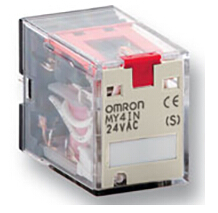 Omron 的 MY 系列继电器包括
人气:139
Omron 的 MY 系列继电器包括
人气:139
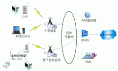 ZSP800是一款宽带无线通信
人气:136
ZSP800是一款宽带无线通信
人气:136
 粤ICP备13004986号-3