


目录
一,产品概述(General Description)
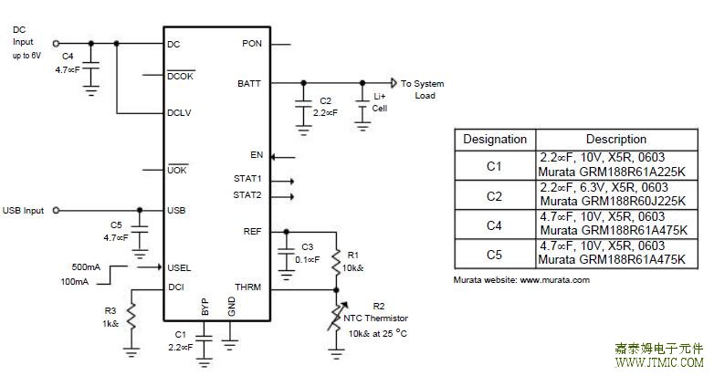
The JTMA3200 charges a single-cell Li+ battery from both
USB and AC adapter sources. It also includes battery-to-input power switchover, therefore, the system can be powered directly from the
power source rather than from the battery.
In its simplest application, the JTMA3200 doesn’t need external MOSFET or diodes and accepts input voltages up to 6.5V; however, DC input over-voltage protection up to 18V can be added with a single SOT PFET.On-chip thermal limiting simplifies PC board layout and allows optimum charging rate without the thermal limits imposed by worst-case battery and input voltage.
When the JTMA3200 thermal limit is reached, the charger does not shut down but simply reduces charging current.Ambient or battery temperature can be monitored with an external thermistor. When the temperature is out of range, charging pauses.Other features include STAT 1 and STAT 2 outputs indicating various charge status. DC
power-OK (DCOK),USB power-OK (UOK), and poweron (PON) outputs
indicate when valid power is present. These outputs drive logic or power-selection MOSFETs to disconnect the charging sources from the load
and to protect the JTMA3200 from overvoltage. The JTMA3200 doesn’t contain logic for communication with the USB host. It must receive instructions from a local microcontroller. The JTMA3200
is available in 16-pin 5mmx5mm QFN and 4mmx4mm TQFN packages and operates over the -40°C to +85°C temperature range.
二.产品特点(Features)
1.)Charge from USB or AC Adapter
2.)Accurate BATT Regulation Voltage
3.)Programmable DC Charging Current
4.)Selectable USB Charging Current (Either 100mA or 500mA)
5.)Thermal Regulation for Simplified Board Design
6.)Input Protection Up to 18V
7.)Soft-Start
8.)External Thermistor Monitoring
9.)Charge Shutdown Control
10.)Charge Status Outputs
11.)DC and USB Power-OK Indicators
12.)Small, High Power QFN5x5-16 and TQFN4x4-16 Packages
13.)Lead Free and Green Devices Available(RoHS Compliant)
三,应用范围 (Applications)
Wireless Appliances
Digital Still Camera
Internet Appliances
Smart Phones and PDAs
四.下载产品资料PDF文档
 |
jtma3200 |
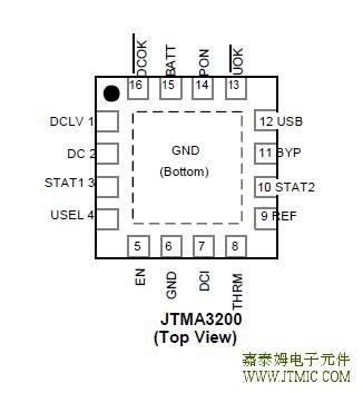
FUNCTION
Enable in Charge Done
| PIN |
FUNCTION Enable in Charge Done |
|
| NO. | NAME | |
| 1 | ||
| DCLV |
DC charger power input from an AC adapter. DCLV charges BATT through an internal MOSFET. Maximum operating voltage at this pin is 6.0V. When an over-voltage protection MOSFET is connected,Enable inDCLVChargeis connectedDoneto DC when the input voltage is suitable for charging. |
|
| 2 | DC |
Voltage-Sense Pin for DC Input from AC Adapter. Maximum operating voltage at this pin is 18V. Enable in Charge Done This voltage-sense function provides status of DC voltage from AC adapter for over-voltage protection. |
| 3 | STAT1 | Charge status output pin 1. This pin is an active-high, open-drain output pin. |
| 4 | USEL |
USB charging current selection input. USEL is a logic input that sets USB source charging current to 500mA when USEL is logic high and to 100mA when USEL is logic low. |
| 5 | EN |
Charging enable/disable control pin. Drive EN high to enable the device. When EN is low, the charger stops charging and DCOK, UOK, and PON remain active. |
| 6 | GND | Signal and power ground. |
| 7 | DCI |
DC charging current setting pin. Connecting a resistor to the GND sets the fast-charge current when the DCLV input is powering the charger. |
| 8 | THRM |
External thermistor connection pin. THRM pauses charging when an externally connected the o o o thermistor (10kΩ at +25 C) is at less than 0 C or greater than +50 C. Connecting this pin to the GND disables this function. |
| 9 | REF |
3V Reference voltage output pin. Sources up to 1.5mA to bias the external thermistor. Bypass with 0.1µF to the GND. REF loading does not affect BATT regulation accuracy. |
| 10 | STAT2 | Charge status output pin 2. This pin is an active-high, open-drain output pin. |
| 11 | BYP |
Bias supply pin for internal circuitry. This pin switches to the pin (either DCLV or USB) with higher supply than the other. Bypass with a 2.2µF capacitor to the GND. |
| 12 | USB | USB charger power input. Charge BATT through an internal MOSFET. |
| 13 | UOK |
USB power-ok output pin. UOK is an active-low, open-drain output that goes low when USB is the valid charging source (VUSB >3.65V and VDC<3.65V). |
| 14 | PON |
Gate driver output pin for the P-channel MOSFET disconnecting battery from system load when power is applied. PON is an active-high, open-drain output with an internal 140kΩ resistor to the ground that goes high when VDC or VUSB is ready. |
| 15 | BATT | Charger output pin. Connect this pin to the positive terminal of a Li+ battery. |
| 16 | DCOK |
DC power-ok output pin. DCOK is an active-low, open-drain output that goes low when 3.65V < VDC < 6.4V. |
| Pad | EP |
Exposed metal pad. This pad is connected to the ground. Note this internal connection is a soft-connect, meaning there is no internal metal or bond wire physically connecting the exposed pad to the GND pin. The connection is through the silicon substrate of the die and then through a conductive epoxy. Connecting the exposed pad to the ground does not remove the requirement for a good ground connection to the GND. |
七,功能概述
Input Overvoltage Protection Switch
Connect a P-channel MOSFET between DCLV and DC to protect the DCLV input pin from over-voltage up to 18V.
When DC voltage is above 6.4V OVP threshold, the DCOK will be pulled high to turn off the P-channel MOSFET. The
P-channel MOSFET will be turned on again until the DC voltage is below the OVP threshold. If the OVP function is
not needed, leave the DCOK open and tie the DC pin to DCLV pin.
Battery-Load Switch
When an AC adapter or USB power is connected to charger, some systems prefer that system load is
supplied from the AC adapter or USB power rather than from the battery. In these systems, the battery is
permanently connected to system load. If the battery is completely discharged, the system might not ready to
operate immediately. If the battery-load switch function is needed, uses external components D1, D2, Q1, Q2, and
Q3 to achieve the function.Typical Application Circuit 3 shows the full-featured circuit.When input power is supplied, the Q1 disconnects the battery from the system load. The input can power the system through D1, D2, Q2, and Q3 when either USB or AC power is present. Typical Application Circuit 4 shows the partial battery-load switching. AC adapter power is routed directly to the battery but USB power is not. When the USB power is connected, total USB current is set by USEL and system power is drawn from the battery through D2.
STAT Pins
The STAT1 and STAT2 outputs indicate various charge status. These two pins can be used to drive LEDs or
communicate to the host processor. When status pins are monitored by a processor, there should be a 10kΩ
pull-up resistor to connect each status pin and the VCC of the processor; furthermore, when the status is viewed by
LED, the LED with a current rating is less than 10mA and a resistor should be selected to connect LED in series,
so the current will be limited to the desired current value. The resistor is calculated by the following equation:
In other words, the LED and resistor between the input and each status pin shoule in series.
Capacitor Selection
Typically, a 4.7µF ceramic capacitor is used to connect from DC/USB to the GND. For high charging current, it is
recommended to use a larger input bypass capacitance to reduce supply noise. Note that if the OVP function is
used, the DC should protect against the high DC input voltage, so the voltage rating of the DC input capacitor
must be larger than 25V.
There is a ceramic capacitor connecting from BATT to the GND for proper stability. To work well with most
applications, at least a 2.2µF X5R ceramic capacitor is required.
Thermal Consideration
The JTMA3200 is available in a thermally enhanced QFN package with an exposed pad. It is recommended to con-
nect the exposed pad to a large copper ground plane on the backside of the circuit board through several ther-
mal vias for heatsinking. The exposed pad transfers heat away from the device, allowing the JTMA3200 to
charge the battery with maximum current while minimiz-ing the increase in die temperature. The most common measure of package thermal perfor-mance is thermal resistance measured from the device junction to the air surrounding the package surface (èJA).The èJA can be calculated by the following equation:
where:
TJ=device junction temperature
TA= ambient temperature
PD=device power dissipation
The device power dissipation, PD, is the function of the
charge rate and the voltage drop across the internal FET.
It can be calculated by the following equation:
PCB Layout Consideration
The JTMA3200 is packaged in a thermally enhanced QFN package. The package includes a thermal pad to provide
an effective thermal contact between the device and the printed circuit board. Connecting the exposed pad to a
large copper ground plane on the backside of the circuit board through several thermal vias for heatsinking is
recommended. Connecting the battery to BATT as close to the device as possible provides accurate battery volt-
age sensing. All decoupling capacitors and filter capaci- tors should be placed as close as possible to the device.
The high-current charge paths into DC, DCLV, USB, and from the BATT pins must short and wide to minimize volt-
age drops.
八,相关产品
| Part_No | Package & Pins | Input Voltage (V) | Quiescent Current (typ)(uA) | Charge Current (max)(A) | Battery Charge Voltage | VIN OVP | USB Input | Battery-Load Switch | Charge State Output | |
| min | max | |||||||||
| JTMA3200 | 4.35 | 6 | 2000 | 1000 | 4.2 | Y | Y | Y | Y | |
| JTMA3201 | DFN3x3-10 | 4.35 | 6 | 2000 | 1000 | 4.2 | N | N | N | Y |
| JTMA3202 | SOT-23-5 | 4.35 | 6 | 300 | 500 | 4.2 | N | N | N | Y |
| JTMA3207 | DFN3x3-10 | 4.35 | 6.5 | 300 | 500 | 4.2 | N | N | N | Y |
 Omron 的 MY 系列继电器包括
人气:139
Omron 的 MY 系列继电器包括
人气:139
 ZSP800是一款宽带无线通信
人气:136
ZSP800是一款宽带无线通信
人气:136
 调频调幅收音机程序IC K
人气:118
调频调幅收音机程序IC K
人气:118
 粤ICP备13004986号-3