


目录
一,产品概述(General Description)
The JTMA7262 combine switch-mode battery charger and a boost regulator with fixed 3MHz switching frequency,which drives two integrated N-channel power MOSFETs.In battery charging, the high-efficiency step-down DC/DCconverter is capable of delivering 1.5A output current over
a wide input voltage range from 4V to 6V for JTMA7262, the step-down DC/DC converter is ideally suited for portable electronic devices that are powered from 1-cell Li-ion battery. The Charging parameters and operating modes can be programmed through an I 2C interface. The
JTMA7262 has high accuracy regulation of input current,charge current and charge voltage. It equipped with charge termination, and charge status monitoring for battery detection.
The JTMA7262 charge the battery in three phases:conditioning, constant current and constant voltage. The JTMA7262 features Dynamic Power Management (DPM) mode to accomplish input power limiting. The input cur-rent is limited to the value set by the I2C host. This feature
reduces battery charge current when the input power limit is reached to avoid overloading the AC adapter when sup-plying the load and the battery charger simultaneously.The charge termination is based on battery voltage, a programmed minimum current level and charge current
termination bit set by the I2C host.If the battery voltage falls below an internal threshold, the JTMA7262 automatically restarts the charge cycle, and when the input voltage falls below the battery voltage, it will enter a low-quiescent current sleep mode. The JTMA7262 supports the thermal regulation and over tem-perature protection to maintain the junction temperature of 120oC by reducing charge current.
The JTMA7262 can operate as a boost regulator. To sup-port USB OTG device, JTMA7262 can provide VBUS (5.05V) by boosting the battery voltage.
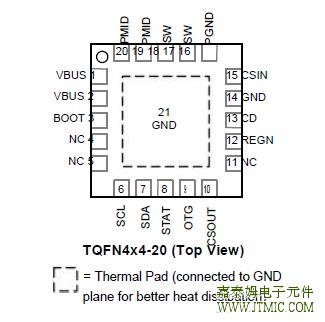
The JTMA7262 is available in1.7mmx2.1mm WLCSP-20 and TQFN4x4-20A packages.
a wide input voltage range from 4V to 6V for JTMA7262, the step-down DC/DC converter is ideally suited for portable electronic devices that are powered from 1-cell Li-ion battery. The Charging parameters and operating modes can be programmed through an I 2C interface. The
JTMA7262 has high accuracy regulation of input current,charge current and charge voltage. It equipped with charge termination, and charge status monitoring for battery detection.
The JTMA7262 charge the battery in three phases:conditioning, constant current and constant voltage. The JTMA7262 features Dynamic Power Management (DPM) mode to accomplish input power limiting. The input cur-rent is limited to the value set by the I2C host. This feature
reduces battery charge current when the input power limit is reached to avoid overloading the AC adapter when sup-plying the load and the battery charger simultaneously.The charge termination is based on battery voltage, a programmed minimum current level and charge current
termination bit set by the I2C host.If the battery voltage falls below an internal threshold, the JTMA7262 automatically restarts the charge cycle, and when the input voltage falls below the battery voltage, it will enter a low-quiescent current sleep mode. The JTMA7262 supports the thermal regulation and over tem-perature protection to maintain the junction temperature of 120oC by reducing charge current.
The JTMA7262 can operate as a boost regulator. To sup-port USB OTG device, JTMA7262 can provide VBUS (5.05V) by boosting the battery voltage.
The JTMA7262 is available in1.7mmx2.1mm WLCSP-20 and TQFN4x4-20A packages.
二.产品特点(Features)
1.)Charge Faster Than Linear Charger
2.)3MHz with 0% to 99.5% Duty Cycle Synchronous
Switch-Mode Charger with 1.5A Integrated N-MOSFETs
3.)4V-6V Input Operating Range
4.)20V Absolute Maximum Input Voltage
5.)Safety
Reverse leakage protection to prevent battery
drainage
Thermal regulation and protection
Input/output over-voltage protection
Cycle-by-cycle current limit
6.)Accuracy
+1% charge voltage regulation (0 to 85oC)
+5% charge current regulation
+5% input current regulation (100mA and500mA)
Built-In Input Current Sensing and Limiting
7.)Automatic Charging
8.)Programmable Through High-Speed I2C
Interface(3.4Mb/s)
Input Current Limit
Fast-Charge and Termination Current
Charge Regulation Voltage
Weak Battery Voltage Threshold
VIN DPM Threshold
Termination Enable/Disable
OTG Enable/Disable
Reset All Parameter Control
Safety Timer with Reset Control
9.)5V, 500mA Boost Mode for USB OTG for 2.5V to
4.5V Battery Input
10.)Available in 1.7mmx2.1mm WLCSP-20 and
TQFN4x4-20A Packages
三,应用范围 (Applications)
Cell Phones, Smart Phones and PDAs
Tablet PC
Portable Media Players, Handheld Device
四.下载产品资料PDF文档
 |
jtm7262 |
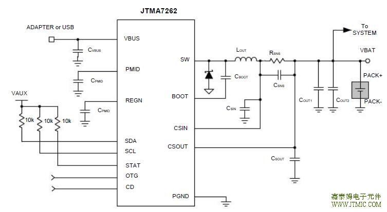
六.电路原理图
七,功能概述
Safety Timer
At the beginning of charging process, the IC starts a 40-minute timer that can be only disabled by VBUS POR
Toggle. When the 40-minute timer times out, the IC turns off the charging operation, set CE bit to 1 (REG1[2]) and
indicates a timer fault (110) on the FAULT bit (REG[2:0]).Toggle POR or write CE bit to 0 can restart charging
process. Fault condition is cleared by POR and fault sta-tus bits can only be updated after the STAT bit are read by
the host.
In default operation condition, 32-second timer is dis-abled and it can be programmable through 32sec timer
bit (REG6[7]). If 32-second timer is enabled, it can be reset by any write-action performed by host through I2C
interface. Writing “1” to reset the TMR_RST bit (REG0[7])will reset the 32-second timer and TMR_RST is auto-
matically set to “0” after the 32-second timer is reset. The charge is terminated and charge parameters are reset to
default values when the 32-second timer expires. Then the 40-minute timer starts and the charge resumes.
Special Charger
The JTMA7262 has additional functionality to limit Input current in case a current-limited “special charger” is sup-
plying VBUS. If VBUS voltage is equal to the programmable VSP (REG5[4]), the PWM controller starts to decrease the
operation frequency and limits the charge current to keep VBUS=VSP.
Safety Settings
The JTMA7262 provides a SAFETY register (REG6) To avoid the value of the IO_CHARGE exceeding from the value
of the ISAFE (REG4[6:4]).
The ISAFE register establishes value that limit the maxi-mum value of IO_CHARGE used by the control logic. If the host
attempts to write a value higher than ISAFE to IO_CHARGE,the ISAFE value as the IO_CHARGE register value.
Input Current Limit
The JTMA7262 integrated the input current sensing circuit and control loop. When operating in boost mode, the in-
put current limit is default 500mA. In charge mode, the input current limit is set by the programmed control bits
in register 01H.
Thermal Regulation
To prevent overheating of the chip during the charging process, the IC monitors the junction temperature, TJ, of
the die. Once TJ reaches the thermal regulation threshold,TCF, the IC begins to taper down the charge current. When
the junction temperature increases approximately 10oC above TCF, the charge current is reduced to zero. In
any state, The IC suspends charging if TJ exceeds TSHTDWN.In thermal shutdown mode, PWM is turned off and all
timers are frozen. When TJ falls below TSHTDWN by approxi-mately 10oC, the JTMA7262 resumes charging process.
Sleep Mode
If the V BUS voltage falls below the sleep mode entry threshold, VCSOUT+VSLP, the IC enters to the sleep mode.
This feature prevents draining the battery during the ab-sence of VBUS. During sleep mode, the internal reverse
blocking switch and PWM controller are turned off.
VBUS Low Voltage Detection (UVLO)
During charging process, the JTMA7262 continuously monitors VBUS voltage. If VBUS falls below UVLO threshold,
the IC stops to charge and sets STAT bits to “11”, the FAULT bits to “011” off. If VBUS rises above UVLO rising threshold, the charging process is repeated.
VBUS Over-Voltage Protection
The IC provides a built-in input over voltage protection (OVP) to protect the device and other components against
damage if the VBUS voltage goes too high. When the VBUS OVP condition is detected, the IC turns off the PWM
converter, sets the STAT bit to “11”and FAULT bits to “001”. Once VBUS drops below the VBUS OVP exit threshold,
the fault is cleared and charge process resumes.
Battery Over-Voltage Protection
The IC provides a built-in over voltage protection to pro- tect the device and other components against damage if
the battery voltage goes too high, as when the battery is suddenly removed. When the battery OVP condition is
detected, the IC turns off the PWM converter, sets the STAT bit to “11” and FAULT bits to “100”.Once VBAT drops to the battery OVP threshold, the fault is cleared and charge process resumes.
八,相关产品
| Part_No | Package & Pins | Input Voltage (V) | Quiescent Current (typ)(uA) | Charge Current (max)(A) | Battery Charge Voltage | VIN OVP | USB Input | Battery-Load Switch | Charge State Output | |
| min | max | |||||||||
| JTMA3200 | 4.35 | 6 | 2000 | 1000 | 4.2 | Y | Y | Y | Y | |
| JTMA3201 | DFN3x3-10 | 4.35 | 6 | 2000 | 1000 | 4.2 | N | N | N | Y |
| JTMA3202 | SOT-23-5 | 4.35 | 6 | 300 | 500 | 4.2 | N | N | N | Y |
| JTMA3207 | DFN3x3-10 | 4.35 | 6.5 | 300 | 500 | 4.2 | N | N | N | Y |
 Omron 的 MY 系列继电器包括
人气:139
Omron 的 MY 系列继电器包括
人气:139
 ZSP800是一款宽带无线通信
人气:136
ZSP800是一款宽带无线通信
人气:136
 调频调幅收音机程序IC K
人气:118
调频调幅收音机程序IC K
人气:118
 粤ICP备13004986号-3