


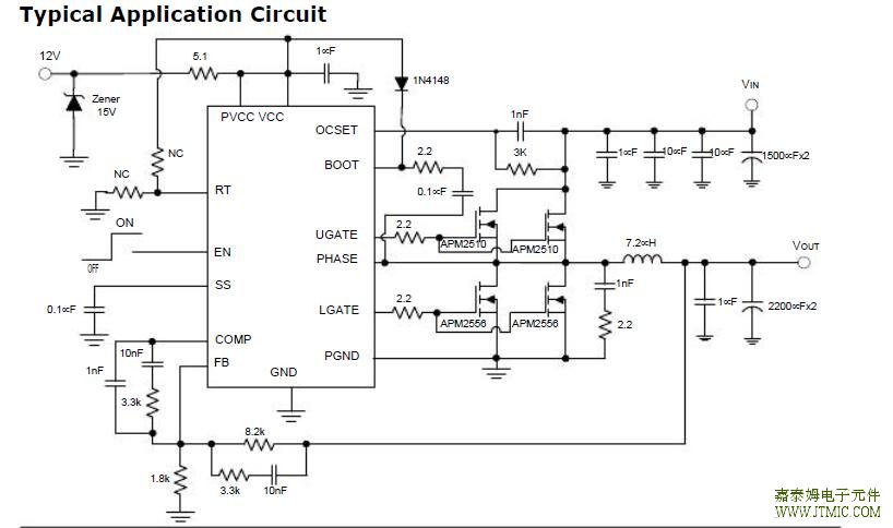
六.电路原理图
七,功能概述
Layout Consideration
In any high switching frequency converter, a correct layout is important to ensure proper operation
of the regulator.With power devices switching at 300kHz,the resulting cur-rent transient will cause
voltage spike across the i n t e r c o n n e c t i n g impedance and parasitic circuit elements. As an
example, consider the turn-off transition of the PWM MOSFET. Before turn-off, the MOSFET is
carrying the full load current. During turn-off, current stops flowing in the MOSFET and is
free-wheeling by the lower MOSFET and parasitic diode. Any parasitic inductance of the circuit
generates a large voltage spike during the switching interval. In general, using short and
wide printed circuit traces should minimize interconnect-ing impedances and the magnitude
of voltage spike.And signal and power grounds are to be kept separating till combined using
the ground plane construction or single point grounding. Figure 10 illustrates the layout,
with bold lines indicating high current paths; these traces must be short and wide. Components
along the bold lines should be placed lose together. Below is a checklist for your layout:
- Keep the switching nodes (UGATE, LGATE, and PHASE) away from sensitive small signal nodes
since these nodes are fast moving signals. Therefore,keep traces to these nodes as short as possible.
- The traces from the gate drivers to the MOSFETs (UGATE, LGATE) should be short and wide.
- Place the source of the high-side MOSFET and the drain of the low-side MOSFET as close as possible.
Minimizing the impedance with wide layout plane between the two pads reduces the voltage bounce of
the node.
- Decoupling capacitor, compensation component, the resistor dividers, boot capacitors, and SS capacitors
should be close their pins. (For example, place the decoupling ceramic capacitor near the drain of the
high-side MOSFET as close as possible. The bulk capacitors are also placed near the drain).
- The input capacitor should be near the drain of the upper MOSFET; the output capacitor should be near
the loads. The input capacitor GND should be close to the output capacitor GND and the lower MOSFET
GND.
- The drain of the MOSFETs (VIN and PHASE nodes)should be a large plane for heat sinking.
 JTM3110B 是 一 款 高 效 、
人气:199
JTM3110B 是 一 款 高 效 、
人气:199
 粤ICP备13004986号-3