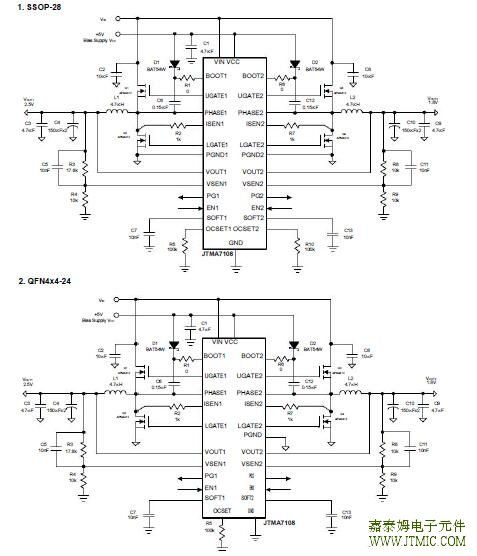
六.电路原理图

七,功能概述
Layout Consideration (Cont.)
· Keep the switching nodes (UGATEx, LGATEx, BOOTx,PHASEx, and ISENx) away from sensitive small sig-
nal nodes since these nodes are fast moving signals.Therefore, keep traces to these nodes as short as
possible and there should be no other weak signal traces in parallel with theses traces on any layer.
· The signals going through theses traces have both high dv/dt and high di/dt, with high peak charging and
discharging current. The traces from the gate drivers to the MOSFETs (UGATEx and LGATEx) should be short
and wide.
· Place the source of the high-side MOSFET and the drain of the low-side MOSFET as close as possible.
Minimizing the impedance with wide layout plane between the two pads reduces the voltage bounce of
the node.
· The ISENx trace should be a separate trace, and independently go to the drain terminal of the low-side
MOSFET. The current sense resistor should be close to ISENx pin. The loop formed by the bottom MOSFET,
output inductor, and output capacitor, should be very small. The source of the bottom MOSFET should tie
to the negative side of the output capacitor in order for the ISENx pin to get the voltage drop on the RDS(ON).
· Decoupling capacitor, compensation component,the resistor dividers, boot capacitors, and soft-start
capacitors should be close their pins. (For example,place the decoupling ceramic capacitor near the drain
of the high-side MOSFET as close as possible. The bulk capacitors are also placed near the drain).
· The input capacitor should be near the drain of the high-side MOSFET; the high quality ceramic
decoupling capacitor can be put close to the VCC and GND pins; the output capacitor should be near the
loads. The input capacitor GND should be close to the output capacitor GND and the low-side MOSFET
GND.
· The drain of the MOSFETs (VIN and PHASEx nodes) should be a large plane for heat sinking. And
PHASEx pin traces are also the return path for UGATEx. Connect these pins to the respective
converter’s high-side MOSFET source.
The JTMA7108 uses ripple mode control. Build the resistor divider close to the VSENx pin so that the
high impedance trace is shorter. The VSENx pin traces can’t be closed to the switching signal traces (UGATEx,
LGATEx, BOOTx, PHASEx, and ISENx).
The PGNDx trace should be a seperate trace, and inpendently go to the source of the low-side MOSFET.
For QFN4x4-24 package only, the thermal pad is the PGND of the dual channels. The sources of the both
channels’ low-side MOSFETs should be near the PGND respectively.


 JTM3110B 是 一 款 高 效 、
人气:199