


Input Capacitors
The JTMA3207 requires proper input capacitors to supply surge current during stepping load transients to prevent
the input rail from dropping. The 1µF ceramic capacitors are recommended to place on the input supply pins (VIN
and VLDOIN) to the GND. Place the capacitors as close as possible to the input supply pins for well operation. In
some start-up conditions, it may necessary to protect the device against a hot plug input voltage. Adding a 6V input
zener diode between the input supply pins and the GND clamps the input voltage peak.
Output Capacitors
The JTMA3207 has two output pins, which are charger output pin BATT and regulator 3.3V output pin LDOOUT.
The output capacitor of charger is recommended to use 2.2µF ceramic capacitor to ensure the battery charge
stability.
The output capacitor of regulator also can use ceramic capacitor, and its proper value is between 1µF and 2.2µF,
ESR must above 10mΩ. Large output capacitor values can reduce noise and improve load-transient response,
stability, and PSRR. With X5R and X7R dielectrics, 1µF is sufficient at all operating temperatures.
STAT Pin
The STAT pin can be used to drive a LED or communicate with the host processor to show the charge status. When
the status is displayed by a LED, which has a current rating less than 5mA, a resistor should be selected to
connect LED in series, for programming at the desired current value. The resistor is calculated by the following
equation:
When STAT pin is monitored by a processor, there should be a 10kΩ to 100kΩ pull-up resistor to connect the STAT
pin and the supply voltage of the processor.
pin and the supply voltage of the processor.
Thermal Consideration
The most common measurement of package thermal performance is thermal resistance measured from the
device junction to the air surrounding the package sur-face (èJA). The èJA can be calculated by the following
equation:
where:
TJ= device junction temperature, maximum TJ=120°C TA= ambient temperature PD= device power dissipation
The device power dissipation, PD, is a function of the charge rate, the LDO output current and the voltages drop
across the internal FETs.It can be calculated by the following equation:
PD = (VIN − VBATT ) × ICHG + (VLODIN − VLDOUT ) × ILDO
PCB Layout Consideration
Connecting the battery to BATT as close as possible pro-vides accurate battery voltage sensing. The input and
output decoupling capacitors and the programmed re-sistor RSET should be placed as close as possible to the
device. The high current paths (VIN and LDOIN pins for input and BATT and LDOOUT pins for output) must be
short and wide to minimize voltage drop.
八,相关产品
| Part_No | Package & Pins | Input Voltage (V) | Quiescent Current (typ)(uA) | Charge Current (max)(A) | Battery Charge Voltage | VIN OVP | USB Input | Battery-Load Switch | Charge State Output | |
| min | max | |||||||||
| JTMA3200 | 4.35 | 6 | 2000 | 1000 | 4.2 | Y | Y | Y | Y | |
| JTMA3201 | DFN3x3-10 | 4.35 | 6 | 2000 | 1000 | 4.2 | N | N | N | Y |
| JTMA3202 | SOT-23-5 | 4.35 | 6 | 300 | 500 | 4.2 | N | N | N | Y |
| JTMA3207 | DFN3x3-10 | 4.35 | 6.5 | 300 | 500 | 4.2 | N | N | N | Y |
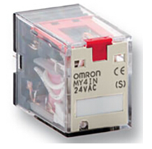 Omron 的 MY 系列继电器包括
人气:139
Omron 的 MY 系列继电器包括
人气:139
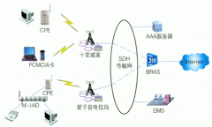 ZSP800是一款宽带无线通信
人气:136
ZSP800是一款宽带无线通信
人气:136
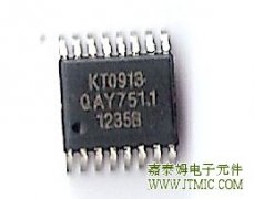 调频调幅收音机程序IC K
人气:118
调频调幅收音机程序IC K
人气:118
 粤ICP备13004986号-3