 中文
中文 English
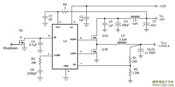
双N通道mosfetCXSD6277/A/B车载直流-直流转换器低成本的同步降压调节器VCC和VC电源的上电复位POR外部可编程软启动检测到输出短路时锁定设备的电压检测
| 产品型号: | CXSD6277/A/B |
| 产品类型: | DC-DC转换器 |
| 产品系列: | Buck降压型芯片 |
| 产品状态: | 量产 |
| 浏览次数: | 40 次 |
产品简介
技术参数
| 输入电压范围 (VIN) | ≤ 5~13.2V |
|---|---|
| 输出电压 (VOUT) | ADJV |
| 输出电流 (IOUT) | 5A |
| 工作频率 | 1500 Hz |
| 转换效率 | 95%% |
| 封装类型 | SOP-8|TSSOP-8 |
| Topology | Buck VM降压型芯片 |
| Control method | No. of PWM Outputs:1 |
| Switching frequency | 1500 |
| Protection | Phase: 1 |
| Features | 静态工作电流 Quiescent Current (typ)(uA):3000 |
| Application | Bias Voltage (typ) (V):5~12 |
| Operating temp | -40℃~125℃ |
| Reference design | 反馈电压Reference Voltage(V):1.25 / 0.8 |
产品详细介绍
目录
1.产品概述 2.产品特点3.应用范围 4.下载产品资料PDF文档
5.产品封装图 6.电路原理图
7.功能概述 8.相关产品
一,产品概述(General Description)
The CXSD6277/A/B series are designed to provide a low cost synchronous
Buck regulator for on-board DC to DC con-verter applications. The CXSD6277/A/B
series together with dual N-channel MOSFETs , provide a
low cost solution for such applications. Each device fea-tures an internal
200/400kHz oscillator, Power-On-Reset (POR) for both VCC and VC supplies,
an external pro-grammable soft-start function as well as output under-
voltage detection that latches off the device when an out-put short is detected.
二.产品特点(Features)
1.)Operating with Single 5V or 12V Input
2.)Drives N-Channel MOSFETs
3.)Simple Single-Loop Control Design
Voltage-Mode PWM Control
Full 0% to 100% Duty Ratio
Fast Transient Response
4.)±2% Output Voltage Accuracy Over Temperature
5.)Under-Voltage Protection for Output
6.)200/400kHz Constant Frequency Operation
200kHz for CXSD6277/A/BB
400kHz for CXSD6277/A/BA
7.)Small size, 8-PIN Package (SOIC or TSSOP)
8.)Lead Free and Green Devices Available (RoHS Compliant)
三,应用范围 (Applications)
Graphics Cards
DDR Memory Power Supply
DDR Memory Termination Voltage
Low-Voltage Distributed Power Supplies
四.下载产品资料PDF文档
需要详细的PDF规格书请扫一扫微信联系我们,还可以获得免费样品以及技术支持!

五,产品封装图 (Package)
FB (Pin 1)
Connect this pin to the output (VOUT) of the PWM con-verter via an external resistor divider to provide a voltage
feedback path for the converter. The output voltage set by the resistor divider is determined using the following
for-where ROUT is the resistor connected from VOUT to FB, and RGND is the resistor connected from FB to
ground.The voltage at this pin is also monitored for Under-Volt-age protection.
VCC (Pin 2)
Connect this pin to input voltage from 5V to 20V. This pin provides the bias for the control circuitry and the
power MOSFET driver (LDRV). The voltage at this pin is monitored for Power-On-Reset (POR) purpose.
LDRV (Pin 3)
Connect this pin to the gate of the low-side power MOSFET. This pin provides the gate drive for the MOSFET.
GND (Pin 4)
Signal and power ground for the IC. All voltage levels are measured with respect to this pin.
HDRV (Pin 5)
Connect this pin to the gate of the high-side power MOSFET. This pin provides the gate drive for the MOSFET.
VC (Pin 6)
This pin provides bias voltage to the high-side MOSFET driver. A bootstrap circuit may be used to pump a boot
voltage for enforcing the driving capability of the gate driver and improving the performance of the MOSFET.
COMP (Pin 7)
This pin is the output of the error amplifier. Add an exter-nal resistor-capacitor network to provide a loop compen-
sation for the PWM converter.
SS (Pin 8)
Connect a capacitor from this pin to ground.This capacitor,along with an internal 20μA current source, sets the soft-
start interval of the PWM converter and prevents the out-puts from overshoot as well as limits the input current.
Pull this pin below 0.5V can shutdown the converter.
六.电路原理图
七,功能概述
|
Profile Feature |
Sn-Pb Eutectic Assembly |
Pb-Free Assembly |
|
Average ramp-up rate |
3°C/second max. |
3°C/second max. |
|
Preheat |
100°C |
150°C |
|
Time maintained above: |
183°C |
217°C |
|
Peak/Classification Temperature (Tp) |
See table 1 |
See table 2 |
|
Time within 5°C of actual |
10-30 seconds |
20-40 seconds |
|
Ramp-down Rate |
6°C/second max. |
6°C/second max. |
|
Time 25°C to Peak Temperature |
6 minutes max. |
8 minutes max. |
八,相关产品 更多同类产品......
|
Switching Regulator > Buck Controller |
||||||||||
|
Part_No |
Package |
Archi tectu |
Phase |
No.of PWM Output |
Output Current (A) |
Input Voltage (V) |
Reference Voltage (V) |
Bias Voltage (V) |
Quiescent Current (uA) |
|
|
min |
max |
|||||||||
|
SOP-14 QSOP-16 QFN4x4-16 |
VM |
1 |
1 |
30 |
2.9 |
13.2 |
0.9 |
12 |
8000 |
|
|
SOP-8 |
VM |
1 |
1 |
20 |
2.9 |
13.2 |
0.8 |
12 |
5000 |
|
|
SOP-8 |
VM |
1 |
1 |
20 |
2.9 |
13.2 |
0.8 |
12 |
5000 |
|
|
QFN4x4-24 |
VM |
2 |
1 |
60 |
3.1 |
13.2 |
0.6 |
12 |
5000 |
|
|
SOP-8 |
VM |
1 |
1 |
20 |
2.2 |
13.2 |
0.8 |
5~12 |
2100 |
|
|
SOP-8 |
VM |
1 |
1 |
20 |
2.2 |
13.2 |
0.8 |
5~12 |
2100 |
|
|
SOP8|TSSOP8 |
VM |
1 |
1 |
5 |
5 |
13.2 |
1.25|0.8 |
5~12 |
3000 |
|
|
SOP-8 |
VM |
1 |
1 |
10 |
3.3 |
5.5 |
0.8 |
5 |
2100 |
|
|
SOP-14 |
VM |
1 |
1 |
10 |
5 |
13.2 |
0.8 |
12 |
2000 |
|
|
TSSOP-24 |QFN5x5-32 |
VM |
1 |
2 |
20 |
5 |
13.2 |
0.6 |
5~12 |
4000 |
|
|
SOP14 QSOP16 QFN-16 |
VM |
1 |
1 |
30 |
2.9 |
13.2 |
0.9 |
12 |
4000 |
|
|
SOP-14 |
VM |
1 |
1 |
30 |
2.2 |
13.2 |
0.6 |
12 |
5000 |
|
|
SOP-14 |
VM |
1 |
1 |
30 |
2.2 |
13.2 |
0.6 |
12 |
5000 |
|
|
SOP-14 |
VM |
1 |
1 |
25 |
2.2 |
13.2 |
0.8 |
12 |
5000 |
|
|
LQFP7x7 48 TQFN7x7-48 |
VM |
1 |
6 |
0.015 |
1.4 |
6.5 |
- |
5 |
1800 |
|
|
TSSOP-24P |
VM |
1 |
2 |
20 |
2.97 |
5.5 |
0.8 |
5~12 |
5000 |
|
|
SOP-14 |
VM |
1 |
1 |
10 |
5 |
13.2 |
0.8 |
12 |
3000 |
|
|
SOP-8-P|DIP-8 |
VM |
1 |
1 |
30 |
2.9 |
13.2 |
1.2 |
12 |
3000 |
|
|
SSOP28 QFN4x4-24 |
VM |
1 |
2 |
20 |
5 |
24 |
0.9 |
5 |
1200 |
|
|
SOP-20 |
VM |
1 |
2 |
20 |
2.2 |
13.2 |
0.6 |
5~12 |
4000 |
|
|
SOP8|DFN3x3-10 |
VM |
1 |
2 |
- |
- |
- |
- |
5~12 |
550 |
|
|
DIP8|SOP-8 |
VM |
1 |
1 |
1 |
1.2 |
9 |
24 |
5 |
9 ~ 24 |
|
|
SSOP16 QFN4x4-16 TQFN3x3-16 |
VM |
1 |
1 |
25 |
3 |
25 |
0.6 |
5 |
1700 |
|
|
TDFN3x3-10 |
COT |
1 |
1 |
25 |
3 |
25 |
0.5 |
5 |
350 |
|
|
QFN4x4-24 |
CM |
2 |
1 |
40 |
4.5 |
13.2 |
0.6 |
5~12 |
4000 |
|
|
SOP8P TDFN3x3-10 |
VM |
1 |
1 |
20 |
3 |
13.2 |
0.8 |
5~12 |
2500 |
|
|
SOP8P |
VM |
1 |
1 |
25 |
3 |
13.2 |
0.6|0.8 |
5~12 |
1200 |
|
|
TDFN3x3-10 |
VM |
1 |
1 |
25 |
4 |
13.2 |
0.8 |
5~12 |
2000 |
|
|
TDFN3x3-10 |
COT |
1 |
1 |
25 |
4.5 |
25 |
0.6 |
5~12 |
80 |
|
|
SOP-8P |
VM |
1 |
1 |
25 |
4.5 |
13.2 |
0.8 |
5~12 |
16000 |
|
|
TQFN3x3-10 |
VM |
1 |
1 |
25 |
4.5 |
13.2 |
0.6 |
5~12 |
2500 |
|
|
TDFN3x3-10 |
COT |
1 |
1 |
30 |
3 |
25 |
0.8 |
5~12 |
2000 |
|
|
TQFN3x3-16 |
COT |
1 |
1 |
30 |
1.8 |
28 |
0.6 |
5 |
600 |
|
|
TQFN 3x3 16 |
COT |
1 |
1 |
30 |
1.8 |
28 |
0.6 |
5 |
600 |
|
|
QFN4x4-24 |
VM |
2 |
1 |
50 |
4.5 |
13.2 |
0.6 |
5~12 |
5000 |
|
|
TQFN4x4-24 |
COT |
1 |
2 |
15 |
6 |
25 |
2 |
N |
550 |
|
|
TQFN4x4-24 |
COT |
1 |
2 |
15 |
6 |
25 |
2 |
N |
550 |
|
|
TQFN4x4-4 TQFN3x3-20 |
COT |
1 |
2 |
20 |
3 |
28 |
0.75 |
5 |
800 |
|
|
TQFN3x3-16 |
COT |
1 |
1 |
20 |
1.8 |
28 |
0.75 |
5 |
400 |
|
|
QFN3.5x3.5-14 TQFN3x3-16 |
COT |
1 |
1 |
20 |
1.8 |
28 |
0.75 |
5 |
400 |
|
|
TQFN3x3-16 |
COT |
1 |
2 |
20 |
1.8 |
28 |
0.75 |
5 |
400 |
|
|
QFN3x3-20 TQFN3x3-16 |
COT |
1 |
2 |
20 |
3 |
28 |
1.8|1.5|0.5 |
5 |
740 |
|
|
TQFN4x4-24 |QFN3x3-20 |
CM |
1 |
2 |
15 |
5 |
28 |
0.5 |
N |
3000 |
|
|
TDFN3x3-10 |
COT |
1 |
1 |
20 |
1.8 |
28 |
0.5 |
5 |
250 |
|
|
TQFN3x3-20 |
COT |
1 |
2 |
15 |
6 |
25 |
2 |
N |
550 |
|
|
TQFN 3x3 20 |
COT |
2 |
2 |
11 |
6 |
25 |
2 |
N |
550 |
|
|
TQFN3x3-20 |
COT |
2 |
2 |
11 |
5.5 |
25 |
2 |
N |
280 |
|
|
QFN4x4-24 |
VM |
2 |
1 |
60 |
3.1 |
13.2 |
0.85 |
12 |
5000 |
|
|
SOP-8P |
VM |
1 |
1 |
20 |
2.9 |
13.2 |
0.8 |
12 |
16000 |
|
|
SOP-20 |
VM |
2 |
2 |
30 |
10 |
13.2 |
1 |
12 |
5000 |
|
|
TDFN3x3-10 |
COT |
1 |
1 |
25 |
1.8 |
28 |
0.7 |
5 |
250 |
|
|
TQFN3x3-20 |
COT |
2 |
1 |
40 |
1.8 |
25 |
REFIN Setting |
5 |
700 |
|
|
QFN 3x3 20 TQFN 3x3 16 |
COT |
1 |
2 |
20 |
3 |
28 |
1.8|1.5 1.35|1.2 0.5 |
5 |
800 |
|
|
TQFN3x3 20 |
COT |
1 |
2 |
15 |
3 |
28 |
0.75 |
5 |
220 |
|
|
TQFN3x3 20 |
COT |
1 |
2 |
15 |
3 |
28 |
0.75 |
5 |
220 |
|
|
TQFN3x3-20 |
COT |
1 |
2 |
20 |
3 |
28 |
0.75 |
5 |
180 |
|

用户评论