


目录
一,产品概述(General Description)
Jtm3113 is a wide input voltage, high efficiency CC and CV step-down DC/DC converter that operates in either CV (Constant Output Voltage) mode or CC (Constant Output Current) mode.
Jtm3113 provides low-ripple power, high efficiency, and excellent transient characteristics.The PWM control circuit is able to the duty ratio linearly forms 0 up to 90%. An over current protection and short circuit protection functions are built outside that it can set by a resistance. An external compensation is easily to system stable;the low ESR output capacitor can be used.With the addition of an internal N-channel Power MOS, a coil, capacitors, and a diode connected externally, these ICs can function as step-down switching regulators. They serve as ideal power supply units for portable devices when coupled with the SOP-8L and SOP-8L-EP packages, providing such outstanding features as low current consumption. Since this converter can accommodate an input oltage up to 40V, it is also suitable for the operation via an AC adapter
二.产品特点(Features)
Perfect Solution for Car Charger
Input Voltage:7V to 40V
High CC accuracy ±5%
High CV accuracy ±2%
Duty ratio:0% to 90% PWM control
Oscillation frequency:
120K Hz for A
250K Hz for B
Thermal Shutdown function.
Short Circuit Protect (SCP).
Built-in internal SW N-channel MOS.
Current mode non-synchronous PWM converter
Cycle to cycle Current Limiting
External current limit setting.
Under Voltage Lockout.
Over Voltage Protection.
三,应用范围 (Applications)
四.下载产品资料PDF文档
 |
JTM3113 |
五,产品封装图 (Package)
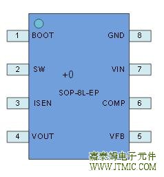
| PIN | NAME | DISCRIPTION |
| 1 | BOOT |
Power to the internal high-side MOSFET gate driver. Connect a 10~100nF capacitor from BS pin to SW pin |
| 2 | SW | Power Switching Output to External Inductor |
| 3 | ISEN | Current Sense Input |
| 4 | VOUT |
Output of DC/DC Converter, Connect To The Anodes Of Output Capacitor |
| 5 | VFB |
The Feedback Of Output Voltage, Connect To The Divider Resistor |
| 6 | COMP |
Error Amplifier Output. This pin is used to compensate the Converter. |
| 7 | VIN |
Power Supply Input. Bypass this pin with a 10μF ceramic capacitor to GND, placed as close to the IC as possible. |
| 8 | GND | Ground |
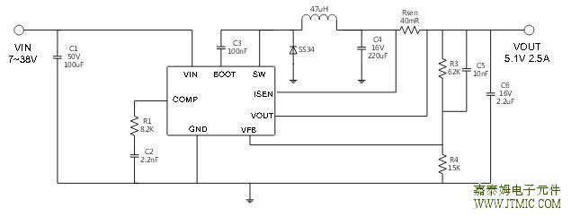
六.电路原理图
七,功能概述
As seen in Functional Block Diagram, the jtm3113 is a peak current mode pulse width modulation
(PWM) converter with CC and CV control. The converter operates as follows:A switching cycle starts when the rising edge of the Oscillator clock output causes the High-Side
Power Switch to turn on. With the SW side of the inductor now connected to Sense1, the inductor
current ramps up to store energy in the magnetic field. The inductor current level is measured by the
Current Sense Amplifier and added to the Oscillator ramp signal. If the resulting summation is higher
than the COMP voltage, the output of the PWM Comparator goes high. When this happens or when
Oscillator clock output goes low, the High-Side Power Switch turns off.
At this point, the SW side of the inductor swings to a diode voltage below ground, causing the
inductor current to decrease and magnetic energy to be transferred to output. This state continues until
the cycle starts again. The High-Side Power Switch is driven by logic using BS as the positive rail. This
pin is charged to VSW + 5V when the Low-Side Power Switch turns on. The COMP voltage is the
integration of the error between FB input and the internal 1V reference. If FB is lower than the reference
voltage, COMP tends to go higher to increase current to the output. Output current will increase until it
reaches the CC limit set by the R1 resistor. At this point, the device will transition from regulating output
voltage to regulating output current, and the output voltage will drop with increasing load.
The Oscillator normally switches at 200KHz. However, if FB voltage is less than 0.45V, then the
switching frequency decreases until it reaches a typical value of 30KHz at VFB = 0.15V
八,相关产品
| DC-DC降压IC | ||||||||||
| 型号 | 输入耐压 | 输出电压 | 输出电流 | 反馈电压 | 工作频率 | 效率 | 静态 | 待机电流 | 封装 | 直接替换 |
| 工作电流 | ||||||||||
| LM2596 | 45V | 5.0V/可调输出 | 3A | 1.23V | 150K | 90% | 10mA | 80uA | TO-263-5L | LM2596/AP1501 |
| /3.3/12V | (Max) | TO-220-5L | ||||||||
| LM2576 | 45V | 5.0V/可调输出 | 3A | 1.23V | 50K | 90% | 10mA | 80uA | TO-263-5L | LM2576 |
| /3.3/12V | (Max) | TO-220-5L | ||||||||
| JTM1507 | 45V | 5.0V/可调输出 | 3A | 1.23V | 380K | 73% | 2mA | 0.2uA | TO-252-5L | AP1507 |
| MP1410 | 27V | 可调输出 | 2A | 1.22V | 420K | 95% | 1mA | 25uA | SOP8 | MP1410/ACT4060 |
| MP9141/RT826 | ||||||||||
| AP1534 | ||||||||||
| JTM1509 | 45V | 5.0V/可调输出 | 2A | 1.23V | 150K | 82% | 2mA | 80uA | SOP8 | AP1509 |
| 3.3V/12V | ||||||||||
| JTM1513 | 20V | 可调输出 | 2A | 0.8V | 150K | 89% | 2mA | 1uA | SOP-8 | AP1513 |
| JTM1530 | 20V | 可调输出 | 3A | 0.8V | 380K | 88% | 3mA | 1uA | SOP-8 | AP1510 |
| JTM1583 | 28V | 可调输出 | 3A | 1.22V | 380K | 89% | 3mA | 1uA | SOP-8 | MP1583 |
| JTM3111 | 42V | 可调输出 | 3A | 0.8V | 50-500K | 91% | 3mA | 150uA | ESOP8 | AX3111 |
| JTM3112 | 40V | 可调输出/ | 2A | 1.18V | 110K | 93% | 10mA | 2mA | SOP8 | |
| 带CC/CV模式 | ||||||||||
| JTM3113B | 40V | 可调输出/ | 2.5A | 1.0V | 250K | 91% | 10mA | 2mA | ESOP8 | |
| 带CC/CV模式 | ||||||||||
| JTM3101 | 45V | 可调输出/ | 2A | 1.235V | 150K | 83% | 2.0mA | ESOP8 | ||
| 带CC模式 | ||||||||||
| JTM3102 | 45V | 可调输出/ | 3A | 1.25V | 150K | 89% | 2.0mA | ESOP8 | ||
| 带CC模式 | ||||||||||
| JTM3109 | 40V | 可调输出/ | 3A | 1.25V | 180K | 89% | 2.1mA | SOP8 | ||
| 带CC/CV模式 | ||||||||||
| JTM3108 | 40V | 可调输出/ | 3.5A | 1.25V | 180K | 87% | 2.1mA | ESOP8 | ||
| 带CC/CV模式 | ||||||||||
| JTM4523 | 40V | 可调输出/ | 3A | 0.8V | 225K | 92% | 2.84mA | 75uA | ESOP8 | AC4523/F5335 |
| 带CC/CV模式 | ||||||||||
| JTM3501 | 50V | 5V固定输出 | 1.8A | 150K | 90% | 4.7mA | SOP-8 | |||
| JTM3511 | 50V | 5V固定输出 | 2.1A | 150K | 90% | 4.7mA | SOP-8 | |||
| JTM3512 | 50V | 5V固定输出 | 2.4A | 150K | 89% | 4.7mA | SOP-8 | |||
| JTM3513 | 50V | 5V固定输出 | 3.2A | 150K | 87% | 4.7mA | TO-252-5L | |||
| 大电流DC-DC降压IC | ||||||||||
| 型号 | 输入耐压 | 输出电压 | 输出电流 | 反馈电压 | 工作频率 | 效率 | 静态工作电流 | 待机电流 | 封装 | 直接替换 |
| JTM3103 | 40V | 可调输出 | 4A | 1.25V | 180K | 94% | 2.1mA | TO-252-5L | ||
| JTM3104 | 36V | 可调输出 | 5A | 1.22V | 240K | 95% | 3.6mA | TO-263-5L | ||
| JTM3105 | 40V | 可调输出 | 5A | 1.25V | 180K | 96% | 2.1mA | TO-263-5L | ||
| JTM3115 | 40V | 可调输出 | 5A | 1.25V | 150K | 86% | 2mA | TO-263-5L | ||
| 带CC/CV模式 | ||||||||||
 JTM3110B 是 一 款 高 效 、
人气:199
JTM3110B 是 一 款 高 效 、
人气:199
 粤ICP备13004986号-3