


目录
一,产品概述(General Description)
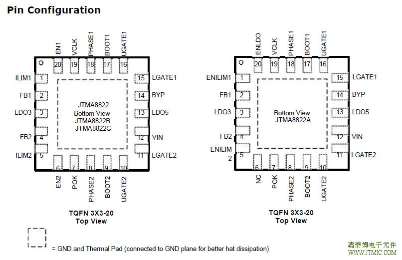
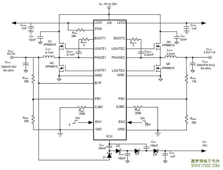
The JTMA8822 JTMA8822A JTMA8822B JTMA8822C integrates dual step-down, constant-on-time,synchronous PWM controllers (that drives dual N-channel MOSFETs for each channel) and two low drop-out regulators as well as various protections into a chip.The PWM controllers step down high voltage of a battery to generate low-voltage for NB applications. The output of PWM1 and PWM2 can be adjusted from 2V to 5.5V by setting a resistive voltage-divider from VOUTx to GND.
The linear regulators provide 5V and 3.3V output for standby power supply. The linear regulators provide up to 100mA output current. When the PWMx output voltage is higher than LDOx bypass threshold, the related LDOx regulator is shut off and its output is connected to VOUTx by internal switchover MOSFET. It can save power dissipation. The charge pump circuit with 270kHz clock driver uses VOUT1 as its power supply to generate ap-proximately 15V DC voltage.
The JTMA8822/A/B/C provides excellent transient response and accurate DC output voltage in either PFM or PWM Mode. In Pulse-Frequency Mode (PFM), the
JTMA8822/A/B/C provides very high efficiency over light to heavy loads with loading-modulated switching frequencies. The Forced-PWM Mode works nearly at
constant frequency for low-noise requirements. The unique ultrasonic mode maintains the switching frequency above 25kHz, which eliminates noise inThe JTMA8822/A/B/C provides excellent transient response and accurate DC output voltage in either PFM or PWM Mode. In Pulse-Frequency Mode (PFM), the
JTMA8822/A/B/C provides very high efficiency over light to heavy loads with loading-modulated switching frequencies. The Forced-PWM Mode works nearly at
audio application.
The JTMA8822/A/B/C is equipped with accurate sourc-ing and current-limit, output under-voltage output over-voltage protections, being perfect for NB applications. A 1.4ms (typ.) digital soft-start can reduce the start-up current. A soft-stop function actively discharges the output capacitors by the discharge device. The JTMA8822/A/B has individual enable controls for each PWM channels. Pulling both EN1/2 pin low shuts down the all of outputs unless LDO3 output. The LDO3 and LDO5 of JTMA8822A/C are always on standby power.
The JTMA8822/A/B/C is available in a TQFN3x3-20 package.
二.产品特点(Features)
Wide Input voltage Range from 6V to 25V
Provide 5 Independent Outputs with ±1.0% Accuracy Over-Temperature
- PWM1 Controller with Adjustable (2V to 5.5V) Out-put
PWM2 Controller with Adjustable (2V to 5.5V) Out-put
100mA Low Dropout Regulator (LDO5) with Fixed 5V Output
100mA Low Dropout Regulator (LDO3) with Fixed 3.3V Output
270kHz Clock Signal for 15V Charge Pump (Used VOUT1 as Its Power Supply)
Excellent Line/Load Regulations about ±1.5% Over-Temperature Range
Built in POR Control Scheme Implemented
Constant On-Time Control Scheme with Frequency
Compensation for PWM Mode
Selectable Switching Frequency in PWM Mode
Built-in Digital Soft-Start for PWM Outputs and Soft-
Stop for PWM Outputs and LDO Outputs
Integrated Bootstrap Forward P-CH MOSFET
High Efficiency over Light to Full Load Range (PWMs)
Built-in Power Good Indicators (PWMs)
Independent Enable Inputs (PWMs, LDO)
70% Under-Voltage and 125% Over-Voltage Protec-tions (PWM)
Adjustable Current-Limit Protection (PWMs)
- Using Sense Low-Side MOSFET’s RDS(ON)
Over-Temperature Protection
3mmx3mm Thin QFN-20 (TQFN3x3-20) package
Lead Free and Green Device Available (RoHS Compliant)
三,应用范围 (Applications)
Notebook and Sub-Notebook Computers
Portable Devices
DDR1, DDR2, and DDR3 Power Supplies
3-Cell and 4-Cell Li+ Battery-Powered Devices
Graphic Cards
Game Consoles
Telecommunications
四.下载产品资料PDF文档
 |
JTMT8822 |
六.电路原理图
 JTM3110B 是 一 款 高 效 、
人气:199
JTM3110B 是 一 款 高 效 、
人气:199
 粤ICP备13004986号-3