


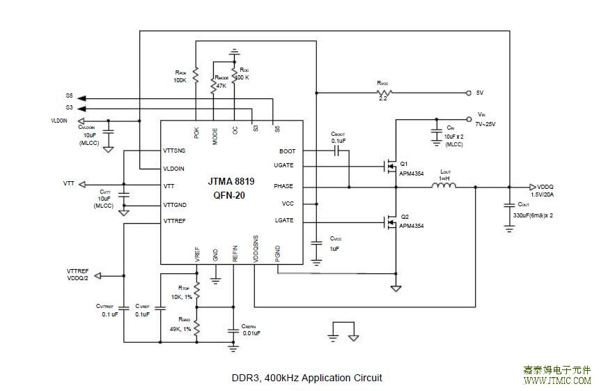
六.电路原理图
七,功能概述
Input Capacitor Selection
The input capacitor is chosen based on the voltage rating and the RMS current rating. For reliable operation, select
the capacitor voltage rating to be at least 1.3 times higher than the maximum input voltage. The maximum RMS
current rating requirement is approximately IOUT/2, where IOUT is the load current. During power up, the input
capaci-tors have to handle large amount of surge current. In low-duty notebook appliactions, ceramic capacitors
are remmended. The capacitors must be connected between the drain of high-side MOSFET and the source of
low-side MOSFET with very low-impeadance PCB layout.
MOSFET Selection
The application for a notebook battery with a maximum voltage of 24V, at least a minimum 30V MOSFETs
should be used. The design has to trade off the gate charge with the RDS(ON) of the MOSFET:
· For the low-side MOSFET, before it is turned on, the body diode has been conducted. The low-side MOSFET
driver will not charge the miller capacitor of this MOSFET.
· In the turning off process of the low-side MOSFET, the load current will shift to the body diode first. The
high dv/dt of the phase node voltage will charge the miller capacitor through the low-side MOSFET driver
sinking current path. This results in much less switching loss of the low-side MOSFETs. The duty
cycle is often very small in high battery voltage applications, and the low-side MOSFET will con-
duct most of the switching cycle; therefore, the RDS(ON) of the low-side MOSFET, the less the power loss. The
gate charge for this MOSFET is usually a secondary consideration. The high-side MOSFET does not have
this zero voltage switching condition, and because it conducts for less time compared to the low-side
MOSFET, the switching loss tends to be dominant. Priority should be given to the MOSFETs with less
gate charge, so that both the gate driver loss and switching loss will be minimized.
The selection of the N-channel power MOSFETs are de-termined by the RDS(ON), reversing transfer capacitance
(CRSS) and maximum output current requirement. The losses in the MOSFETs have two components: conduc-
tion loss and transition loss
Layout Consideration
In any high switching frequency converter, a correct layout is important to ensure proper operation of the regulator.
With power devices switching at higher frequency, the resulting current transient will cause voltage spike across
the interconnecting impedance and parasitic circuit elements. As an example, consider the turn-off transition
of the PWM MOSFET. Before turn-off condition, the MOSFET is carrying the full load current. During turn-off,
current stops flowing in the MOSFET and is freewheeling by the lower MOSFET and parasitic diode. Any parasitic
inductance of the circuit generates a large voltage spike during the switching interval. In general, using short and
wide printed circuit traces should minimize interconnect-ing impedances and the magnitude of voltage spike. And
signal and power grounds are to be kept separating and finally combined to use the ground plane construction or
single point grounding. The best tie-point between the signal ground and the power ground is at the negative
side of the output capacitor on each channel, where there is less noise. Noisy traces beneath the IC are not
recommended
 JTM3110B 是 一 款 高 效 、
人气:199
JTM3110B 是 一 款 高 效 、
人气:199
 粤ICP备13004986号-3