


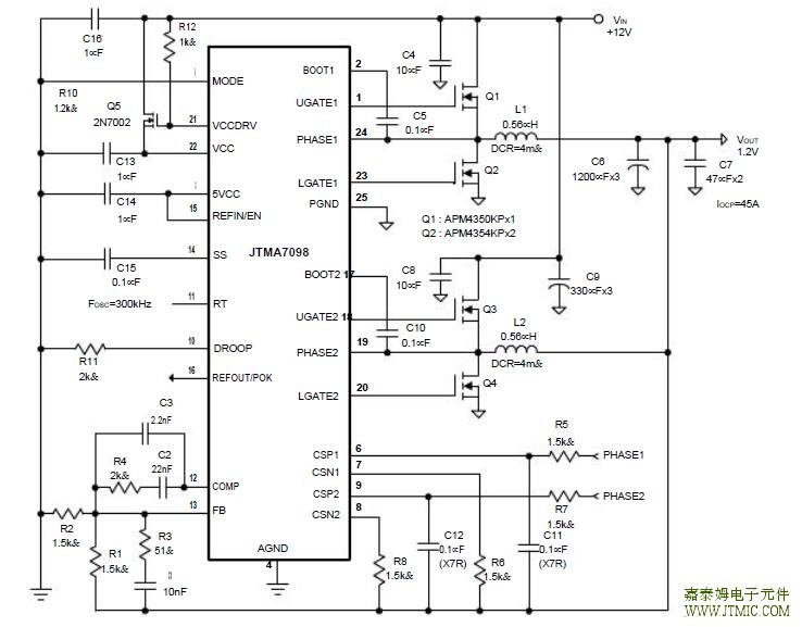
FUNCTION
| PIN | FUNCTION | |
| NO. | NAME | |
| 1 | ||
| UGATE1 |
High-side Gate Driver Output for channel 1. Connect this pin to the gate of high-side MOSFET. This pin is monitored by the adaptive shoot-through protection circuitry to determine when the high-side MOSFET has turned off. |
|
| 2 | BOOT1 |
Bootstrap Supply for the floating high-side gate driver of channel 1. Connect the Bootstrap capacitor between the BOOT1 pin and the PHASE1 pin to form a bootstrap circuit. The bootstrap capacitor provides the charge to turn on the high-side MOSFET. Typical values for CBOOT ranged from 0.1µF to 1µF. Ensure that CBOOT is placed near the IC. |
| 3 | 5VCC |
Internal Regulator Output. This is the output pin of the linear regulator, which is converting power from VCC and provides output current up to 20mA minimums for internal bias and external usage. |
| 4 | AGND |
Signal Ground for the IC. All voltage levels are measured with respect to this pin. Tie this pin to the ground island/plane through the lowest impedance connection available. |
| 5 | MODE |
Operation Phase Selection Input. Pulling this pin lower than 0.64V sets two-phase operation with both channels enabled. Pulling this pin higher than 0.8V sets single-phase operation with the channel 2 disabled. Once operating in single-phase mode, the operation mode is latched. It is required to toggle SS, REFIN/EN, or 5VCC pin to reset the IC. |
| 6 | CSP1 |
Positive Input of current sensing Amplifier for channel 1. This pin combined with CSN1 senses the inductor current through an RC network. |
| 7 | CSN1 |
Negative Input of current sensing amplifier for channel 1. This pin combined with CSP1 senses the inductor current through an RC network. |
| 8 | CSN2 |
Negative Input of current sensing amplifier for channel 2. This pin combined with CSP2 senses the inductor current through an RC network. |
| 9 | CSP2 |
Positive Input of current sensing Amplifier for Channel 2. This pin combined with CSN2 senses the inductor current through an RC network. |
FUNCTION
| PIN | FUNCTION | ||
| NO. | NAME | ||
| 10 | |||
| DROOP |
Load Line (droop) Setting. Connect a resistor between this pin and AGND to set the droop. A sourcing current, proportional to output current is present on the DROOP pin. The droop scale factor is set by the resistors (connected with CSP1, CSP2, and DROOP), resistance of the output inductors, and the internal voltage divider with the ratio of 5%. |
||
| 11 | RT |
Operating Frequency Setting. The three-level input pin sets the operating frequency for each channel. |
|
| RT | Operating Frequency (kHz) | ||
| GND | 150 | ||
| Floating | 300 | ||
| 5VCC | 400 | ||
| 12 | COMP |
Error Amplifier Output. Connect the compensation network between COMP, FB, and VOUT for Type 2 or Type 3 feedback compensation. |
|
| 13 | FB |
Feedback Voltage. This pin is the inverting input to the error comparator. A resistor divider from the output to the AGND is used to set the regulation voltage. |
|
| 14 | SS |
Soft-start Current Output. Connect a capacitor from this pin to the AGND to set the soft-start interval. Pulling the voltage on this pin below 0.5V causes COMP to pull low and then shuts off the output. |
|
| 15 | REFIN/EN |
External Reference and Enable Input. The IC uses the voltage (VREFIN/EN) as reference voltage of the converter with soft-start control. If this pin is driven by an external voltage ranged from 0.4V to 2V. The IC is disabled if the voltage is below 0.4V (typical). If external reference is not available, then connect this pin to 5VCC for internal 0.6V reference. |
|
| 16 |
REFOUT/PO K |
Power-OK and 1.5V Reference Output. This pin is a reference output used to indicate the status of the voltages on SS pin and FB pin. REFOUT/POK provides 1.5V reference if VFB> 87.5% of reference (VR). |
|
| 17 | BOOT2 |
Bootstrap Supply for the floating high-side gate driver of channel 2. Connect the Bootstrap capacitor between the BOOT2 pin and the PHASE2 pin to form a bootstrap circuit. The bootstrap capacitor provides the charge to turn on the high-side MOSFET. Typical values for CBOOT range from 0.1µF to 1µF. Ensure that CBOOT is placed near the IC. |
|
| 18 | UGATE2 |
High-side Gate Driver Output for Channel 2. Connect this pin to the gate of high-side MOSFET. This pin is monitored by the adaptive shoot-through protection circuitry to determine when the high-side MOSFET has turned off. |
|
| 19 | PHASE2 |
Switch Node for Channel 2. Connect this pin to the source of high-side MOSFET and the drain of the low-side MOSFET. This pin is used as sink for UGATE2 driver. This pin is also monitored by the adaptive shoot-through protection circuitry to determine when the high-side MOSFET has turned off. An Schottky diode between this pin and the ground is recommended to reduce negative transient voltage that is common in a power supply system. |
|
| 20 | LGATE2 |
Low-side Gate Driver Output for Channel 2. Connect this pin to the gate of low-side MOSFET. This pin is monitored by the adaptive shoot-through protection circuitry to determine when the low-side MOSFET has turned off. |
|
| 21 | VCCDRV |
Drive for External Linear Regulator. This pin is the drive output for the external linear regulator. Connect this pin to base/gate of NPN/NMOS transistor as the pass element. |
|
| 22 | VCC |
Supply Voltage. This pin along with VCCDRV pin and external pass element provides 8.5V regulated bias supply, low-side gate drivers, and the bootstrap circuit for high-side drivers. This pin can receive a well-decoupled 8V~13.2V supply voltage alone if the VCCDRV is left open. Ensure that this pin is bypassed by a ceramic capacitor next to the pin. |
|
| 23 | LGATE1 |
Low-side Gate Driver Output for Channel 1. Connect this pin to the gate of low-side MOSFET. This pin is monitored by the adaptive shoot-through protection circuitry to determine when the low-side MOSFET has turned off. |
|
| PIN | FUNCTION | |
| NO. | NAME | |
| 24 | ||
| PHASE1 |
Switch Node for Channel 1. Connect this pin to the source of high-side MOSFET and the drain of the low-side MOSFET. This pin is used as sink for UGATT1 driver. This pin is also monitored by the adaptive shoot-through protection circuitry to determine when the high-side MOSFET has turned off. An Schottky diode between this pin and the ground is recommended to reduce negative transient voltage, which is common in a power supply system. |
|
| 25 | PGND |
Power Ground for the low-side gate drivers. Connect this pin to the source of low-side MOSFETs. This pin is used as sink for LGATE1 and LGATE2 drivers. |
 Omron 的 MY 系列继电器包括
人气:139
Omron 的 MY 系列继电器包括
人气:139
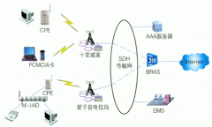 ZSP800是一款宽带无线通信
人气:136
ZSP800是一款宽带无线通信
人气:136
 调频调幅收音机程序IC K
人气:118
调频调幅收音机程序IC K
人气:118
 粤ICP备13004986号-3