


Output Inductor Selection (Cont.)
caused by the AC peak-to-peak sum of the inductor’s current. The ripple voltage of output capacitors can be
caused by the AC peak-to-peak sum of the inductor’s current. The ripple voltage of output capacitors can be
represented by:
For two-phase converter, the inductor value (L) determines the sum of the two inductor ripple currents, ∆IP-P, and af-fects the load transient reponse. Higher inductor value reduces the output capacitors’ripple current and induces
lower output ripple voltage. The ripple current can be approxminated by:
Where F SW is the switching frequency of the regulator.Although the inductor value and frequency are increased
and the ripple current and voltage are reduced, a tradeoff exists between the inductor’s ripple current and the regu-
lator load transient response time.
A smaller inductor will give the regulator a faster load tran-sient response at the expense of higher ripple current.
Increasing the switching frequency (F SW) also reduces the ripple current and voltage, but it will increase the
switching loss of the MOSFETs and the power dissipa-tion of the converter. The maximum ripple current oc-
curs at the maximum input voltage. A good starting point is to choose the ripple current to be approximately 30%
of the maximum output current. Once the inductance value has been chosen, select an inductor that is capable of
carrying the required peak current without going into saturation. In some types of inductors, especially core
that is made of ferrite, the ripple current will increase abruptly when it saturates. This results in a larger out-
put ripple voltage.
Output Capacitor Selection
Output voltage ripple and the transient voltage de-viation are factors that have to be taken into con-
sideration when selecting output capacitors. Higher capacitor value and lower ESR reduce the output ripple
and the load transient drop. Therefore, selecting high performance low ESR capacitors is recommended for
switching regulator applications. In addition to high fre-quency noise related to MOSFET turn-on and turn-off,
the output voltage ripple includes the capacitance voltage drop ∆VCOUT and ESR voltage drop ∆V ESR
∆IP − P
8 × COUT × FSW
∆VESR = ∆IP − P × RESR
These two components constitute a large portion of the total output voltage ripple. In some applications, multiple
capacitors have to be paralleled to achieve the desired ESR value. If the output of the converter has to support
another load with high pulsating current, more capaci-tors are needed in order to reduce the equivalent ESR
and suppress the voltage ripple to a tolerable level. A small decoupling capacitor in parallel for bypassing
the noise is also recommended, and the voltage rating of the output capacitors are also must be considered.
To support a load transient that is faster than the switching frequency, more capacitors are needed for
reducing the voltage excursion during load step change.For getting same load transient response, the output
capacitance of two-phase converter only needs around half of output capacitance of single-phase converter.
Another aspect of the capacitor selection is that the total AC current going through the capacitors has to be
less than the rated RMS current specified on the ca-pacitors in order to prevent the capacitor from over-
heating.
Input Capacitor Selection
Use small ceramic capacitors for high frequency decoupling and bulk capacitors to supply the surge cur-
rent needed each time high-side MOSFET turns on. Place the small ceramic capacitors physically close to the
MOSFETs and between the drain of high-side MOSFET and the source of low-side MOSFET.
The important parameters for the bulk input capacitor are the voltage rating and the RMS current rating. For reliable
operation, select the bulk capacitor with voltage and cur- rent ratings above the maximum input voltage and larg-
est RMS current required by the circuit. The capacitor volt-age rating should be at least 1.25 times greater than the
maximum input voltage and a voltage rating of 1.5 times is a conservative guideline. For two-phase converter, the
MOSFET Selection
The JTMA7098 requires two N-Channel power MOSFETs on each phase. These should be selected based upon
RDS(ON), gate supply requirements, and thermal manage-ment requirements.In high-current applications, the MOSFET power dissipation, package selection, and heatsink are the domi-nant design factors. The power dissipation includes two
loss components, conduction loss, and switching loss.The conduction losses are the largest component of
power dissipation for both the high-side and the low-side MOSFETs. These losses are distributed between
the two MOSFETs according to duty factor (see the equa-tions below). Only the high-side MOSFET has switching
losses since the low-side MOSFETs body diode or an external Schottky rectifier across the lower MOSFET
clamps the switching node before the synchronous rec-tifier turns on. These equations assume linear voltage-
current transitions and do not adequately model powerloss due the reverse-recovery of the low-side MOSFET
body diode. The gate-charge losses are dissipated by the JTMA7098 and don’t heat the MOSFETs. However,
large gate-charge increases the switching interval, tSW which increases the high-side MOSFET switching
losses. Ensure that all MOSFETs are within their maxi-mum junction temperature at high ambient temperature
by calculating the temperature rise according to packagethermal-resistance specifications. A separate heatsink
may be necessary depending upon MOSFET power,package type, ambient temperature and air flow.
For the high-side and low-side MOSFETs, the losses areapproximately given by the following equations:
FSW is the switching frequencytSW is the switching intervalD is the duty cycle Note that both MOSFETs have conduction losses while the high-side MOSFET includes an additional transi-tion loss. The switching interval, t SW, is the function of
the reverse transfer capacitance CRSS. The (1+TC) term isa factor in the temperature dependency of the RDS(ON) and
can be extracted from the “RDS(ON) vs. Temperature”curve of the power MOSFET.
Layout Consideration
In any high switching frequency converter, a correct layout is important to ensure proper operation of the regulator.
With power devices switching at higher frequency, the resulting current transient will cause voltage spike across
the interconnecting impedance and parasitic circuit elements. As an example, consider the turn-off transition
of the PWM MOSFET. Before turn-off condition, the MOSFET is carrying the full load current. During turn-off,
current stops flowing in the MOSFET and is freewheeling by the low side MOSFET and parasitic diode. Any parasitic
inductance of the circuit generates a large voltage spike during the switching interval. In general, using short and
wide printed circuit traces should minimize interconnect-ing impedances and the magnitude of voltage spike.
Besides, signal and power grounds are to be kept sepa-rating and finally combined using ground plane construc-
tion or single point grounding. The best tie-point betweenthe signal ground and the power ground is at the nega-
tive side of the output capacitor on each channel, where there is less noise. Noisy traces beneath the IC are not
recommended. Figure 10. illustrates the layout, with bold lines indicating high current paths; these traces must be
short and wide. Components along the bold lines should be placed lose together. Below is a checklist for your
layout:
 Omron 的 MY 系列继电器包括
人气:139
Omron 的 MY 系列继电器包括
人气:139
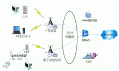 ZSP800是一款宽带无线通信
人气:136
ZSP800是一款宽带无线通信
人气:136
 调频调幅收音机程序IC K
人气:118
调频调幅收音机程序IC K
人气:118
 粤ICP备13004986号-3