 中文
中文 English
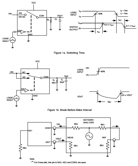
CXES4272高密度双极/双掷DPDT模拟开关它允许-0.3V到+5.5V的信号在电源低于信号范围时无失真通过支持负音频和视频信号模拟信号端口都能承受-0.3V到+5.5V的信号
| 产品型号: | CXES4272 |
| 产品类型: | DC-DC转换器 |
| 产品系列: | 模拟负载开关 |
| 产品状态: | 量产 |
| 浏览次数: | 112 次 |
产品简介
·–支持负音频和视频信号
–-0.3V至+5.5V模拟信号范围,独立于VCC
–导通电阻0.2W(典型值)
–+2.9V至+5.5V单电源范围
–点击弹出抑制
·平滑切换
–进行操作前休息
·2.9V时的低供电电流30mA(典型值)
–可由GPIO供电
–未使用VCC时的高阻抗模式
·NC和NO–+15kV人体模型的ESD保护
技术参数
| 输入电压范围 (VIN) | 2.9~5.5V |
|---|---|
| 输出电流 (IOUT) | 35mA |
| 封装类型 | WLCSP1.2x1.2-9 |
| Topology | 模拟负载开关 |
| Protections | ovp/ocp/otp/scp |
| Control method | 线性 |
| Reaction time(min) | 1ms |
| Internal resistance | 0.2Ω |
产品详细介绍
目录
7.相关产品
产品概述 返回TOP
The CXES4272 is a high-density, double-pole/ doublethrow (DPDT) analog switch which allows signals from - 0.3V to +5.5V to pass without distortion even when the power supply is below the signal range. The low RON resistance (0.2W) makes the devices ideal for low-distortion switching, such as audio. The CXES4272 has internal shunt switches that discharge the audio amplifier AC-coupling capacitance at the normally open (NO1 and NO2) terminals. This feature reduces click-and-pop sounds that occur when switching audio signals between precharged points. The switches are fully specified to operate from a single +2.9V to +5.5V power supply. Because of the low supply current requirement, VCC can be provided by a GPIO. When the power is not applied, switches go to a high-impedance mode and all analog signal ports can withstand signals from -0.3V to +5.5V. The devices control the switches with a control bit, CB. The CXES4272 is available in a 1.2mm x 1.2mm, 0.4mm pitch, 9-bump wafer-level package (WLCSP), and operate over the -4oC to +85oC extended temperature range.
产品特点 返回TOP
· – Negative Audio and Video Signal Capable
– -0.3V to +5.5V Analog Signal Range Independent from VCC
– On-Resistance 0.2W (typ)
– +2.9V to +5.5V Single-Supply Range
– Click-and-Pop Suppression
· Smooth Switch Transition
– Break-Before-Make Operation
· Low Supply Current 30mA (typ) at 2.9V
– Can be Powered by a GPIO
– High-Impedance Mode When VCC Not Applied
· ESD Protection on NC_ and NO_ – +15kV Human Body Model
· WLCSP1.2x1.2-9 (1.2mm x 1.2mm) Package
· 40o C to +85o C Operating Temperature Range
应用范围 返回TOP
· Smartphones
· Tablets
· Portable Audio/Video Equipment
· Portable Navigation Devices
技术规格书(产品PDF) 返回TOP
需要详细的PDF规格书请扫一扫微信联系我们,还可以获得免费样品以及技术支持!

产品封装图 返回TOP


电路原理图 返回TOP


相关芯片选择指南 返回TOP 更多同类产品......
|
Products > Switch > Power Distribution Controller |
|||||||||||||||
|
Part_No |
Package |
No.of Channel |
External Power Switch Type |
Input Voltage (V) |
Quescint Current (uA) |
Wrong Input Voltage Protection |
Inpute Voltage UVLO |
SCP |
OCP (A) |
OVP |
UVP |
EN |
High/ Low EN |
POK |
|
|
min |
max |
||||||||||||||
|
SOP8 TDFN2x2-8 |
1 |
N-Channel MOSFET |
10 |
26 |
750 |
Y |
Y |
Y |
Y |
Y |
Y |
Y |
H |
Y |
|
|
TDFN3x3-10 |
1 |
N-Channel MOSFET |
5 |
26 |
500 |
Y |
Y |
Y |
Y |
Y |
Y |
H |
Y |
||
|
TDFN3x3-10 |
1 |
N-channel MOSFET |
5 |
26 |
500 |
Y |
Y |
Y |
Y |
Y |
Y |
H |
Y |
||
|
Switch> Analog Switch |
||||||||
|
Part_No |
Package & Pins |
VDD Voltage (V) |
IDD, Supply Current (mA) |
Input Voltage (max)(V) |
Power Switch On Resistance(milohm) |
Turn-On Time(ms) |
Turn-Off Time(ms) |
|
|
min |
max |
|||||||
|
WLCSP1.2x1.2-9 |
2.9 |
5.5 |
35 |
0~5.5 |
0.2 |
5 |
1 |
|
|
WLCSP1.2x0.8-6 |
1.5 |
5.5 |
20 |
1.5-5.5 |
22 |
4.4 |
36.5 |
|
|
WLCSP 1.42x0.92-6 |
1.7 |
3.6 |
0.5 |
VDD-5.5~VDD |
0.2 |
0.1 |
1 |
|
|
Switch> DrMOS |
||||||||||||||
|
Part_No |
Package |
Description |
Topology |
# of PWM Outputs |
Drive Lout (A) |
Vin (V) |
Fmax (Khz) |
R-Top (milohm) |
R-Sync (milohm) |
Iq (No load) (uA) |
En pin |
Sync Pin |
PSM/ CCM pin |
|
|
min |
max |
|||||||||||||
|
TQFN4 x4-23P |
High-Performance, High-Current DrMOS Power Module |
high/Low-sideN-channel MOSFET |
1 |
8 |
4.5 |
25 |
1500 |
25 |
7 |
90 |
Y |
N |
Y |
|
|
TQFN4x4 -23P |
High-Performance, High-Current DrMOS Power Module |
high/Low-sideN-channel MOSFET |
1 |
6 |
4.5 |
25 |
1500 |
30 |
12 |
90 |
Y |
N |
Y |
|
|
TQFN5 x5-30 |
High-Performance,High-Current DrMOS Power Module |
high/Low-sideN-channel |
MOSFET1 |
13 |
4.5 |
25 |
1500 |
9.7 |
5.2 |
90 |
Y |
N |
Y |
|
|
TQFN5 x5-30 |
High-Performance,High-Current DrMOS Power Module |
high/Low-sideN-channel MOSFET |
1 |
15 |
4.5 |
25 |
1500 |
8 |
4.5 |
90 |
Y |
N |
Y |
|
|
TQFN5 x5-30 |
High-Performance,High-Current DrMOS Power Module |
high/Low-sideN-channel MOSFET |
1 |
15 |
4.5 |
25 |
1500 |
8 |
4.5 |
90 |
Y |
N |
Y |
|

用户评论