 中文
中文 English
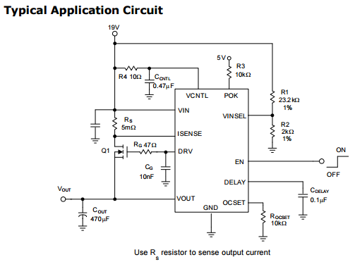
CXES4271 CXES4271A用于外部N沟道MOSFET的高端驱动器允许12V 19V或5V电源导轨错误的输入电压保护功能保护错误的输入适配器插入当输入电压超出目标输入电压范围时IC关闭设备监测VOUT电压以进行短路检测检测到短路
| 产品型号: | CXES4271 |
| 产品类型: | DC-DC转换器 |
| 产品系列: | 模拟负载开关 |
| 产品状态: | 量产 |
| 浏览次数: | 111 次 |
产品简介
·用于外部N沟道MOSFET的高端驱动器
·欠压锁定(UVLO)
·错误的车辆识别号输入电压保护
·输出欠压保护(UVP)
·通电期间的短路保护(SCP)
·过电流保护(OCP)
·可选择的车辆识别号监视器电压
·关闭功能
·电源正常(POK)功能
·提供无铅和绿色设备(符合RoHS)
技术参数
| 输入电压范围 (VIN) | 5~26V |
|---|---|
| 封装类型 | TDFN3x3-10 |
| Iq | 500μA |
| Topology | 模拟负载开关 |
| Protections | ovp/ocp/otp/scp |
| Control method | 线性 |
| Number of channels | 1 |
产品详细介绍
目录
7.相关产品
产品概述 返回TOP
CXES4271A CXES4271 is a high-side power distribution controller for an external N-channel MOSFET, allow for +12V, +19V or +5V power-supply rail. The wrong input voltage protection function protects a wrong input adapter insertion, when input voltage is out of the target input voltage range the IC is off. The over-current protection monitors the output current by using the voltage drop across the external sensing resistor, when output current reaches the trip point the IC will be shut down. The CXES4271A CXES4271 also provides a shortcircuit protection during power-up. The device monitors VOUT voltages for a short-circuit detection, if a short-circuit condition is detected the IC will be shut down. Other features include a POK output to indicate the output voltage is ready, and a logic-controlled shutdown mode.
产品特点 返回TOP
· High-Side Driver for an External N-Channel MOSFET
· Under-Voltage Lockout (UVLO)
· Wrong VIN Input Voltage Protection
· Output Under-Voltage Protection (UVP)
· Short-Circuit Protection During Power-up (SCP)
· Over-Current Protection (OCP)
· Selectable VIN Monitor Voltage
· Shutdown Function
· Power Okay (POK) Function
· Lead Free and Green Devices Available (RoHS Compliant)
应用范围 返回TOP
· AIO Computers
· Notebooks
技术规格书(产品PDF) 返回TOP
需要详细的PDF规格书请扫一扫微信联系我们,还可以获得免费样品以及技术支持!

产品封装图 返回TOP


电路原理图 返回TOP

相关芯片选择指南 返回TOP 更多同类产品......
|
Products > Switch > Power Distribution Controller |
|||||||||||||||
|
Part_No |
Package |
No.of Channel |
External Power Switch Type |
Input Voltage (V) |
Quescint Current (uA) |
Wrong Input Voltage Protection |
Inpute Voltage UVLO |
SCP |
OCP (A) |
OVP |
UVP |
EN |
High/ Low EN |
POK |
|
|
min |
max |
||||||||||||||
|
SOP8 TDFN2x2-8 |
1 |
N-Channel MOSFET |
10 |
26 |
750 |
Y |
Y |
Y |
Y |
Y |
Y |
Y |
H |
Y |
|
|
TDFN3x3-10 |
1 |
N-Channel MOSFET |
5 |
26 |
500 |
Y |
Y |
Y |
Y |
Y |
Y |
H |
Y |
||
|
TDFN3x3-10 |
1 |
N-channel MOSFET |
5 |
26 |
500 |
Y |
Y |
Y |
Y |
Y |
Y |
H |
Y |
||
|
Switch> Analog Switch |
||||||||
|
Part_No |
Package & Pins |
VDD Voltage (V) |
IDD, Supply Current (mA) |
Input Voltage (max)(V) |
Power Switch On Resistance(milohm) |
Turn-On Time(ms) |
Turn-Off Time(ms) |
|
|
min |
max |
|||||||
|
WLCSP1.2x1.2-9 |
2.9 |
5.5 |
35 |
0~5.5 |
0.2 |
5 |
1 |
|
|
WLCSP1.2x0.8-6 |
1.5 |
5.5 |
20 |
1.5-5.5 |
22 |
4.4 |
36.5 |
|
|
WLCSP 1.42x0.92-6 |
1.7 |
3.6 |
0.5 |
VDD-5.5~VDD |
0.2 |
0.1 |
1 |
|
|
Switch> DrMOS |
||||||||||||||
|
Part_No |
Package |
Description |
Topology |
# of PWM Outputs |
Drive Lout (A) |
Vin (V) |
Fmax (Khz) |
R-Top (milohm) |
R-Sync (milohm) |
Iq (No load) (uA) |
En pin |
Sync Pin |
PSM/ CCM pin |
|
|
min |
max |
|||||||||||||
|
TQFN4x 4-23P |
High-Performance, High-Current DrMOS Power Module |
high/Low-sideN-channel MOSFET |
1 |
8 |
4.5 |
25 |
1500 |
25 |
7 |
90 |
Y |
N |
Y |
|
|
TQFN4x 4-23P |
High-Performance, High-Current DrMOS Power Module |
high/Low-sideN-channel MOSFET |
1 |
6 |
4.5 |
25 |
1500 |
30 |
12 |
90 |
Y |
N |
Y |
|
|
TQFN5x 5-30 |
High-Performance,High-Current DrMOS Power Module |
high/Low-sideN-channel |
MOSFET1 |
13 |
4.5 |
25 |
1500 |
9.7 |
5.2 |
90 |
Y |
N |
Y |
|
|
TQFN5x 5-30 |
High-Performance,High-Current DrMOS Power Module |
high/Low-sideN-channel MOSFET |
1 |
15 |
4.5 |
25 |
1500 |
8 |
4.5 |
90 |
Y |
N |
Y |
|
|
TQFN5x 5-30 |
High-Performance,High-Current DrMOS Power Module |
high/Low-sideN-channel MOSFET |
1 |
15 |
4.5 |
25 |
1500 |
8 |
4.5 |
90 |
Y |
N |
Y |
|

用户评论