 中文
中文 English
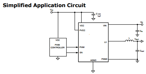
CXES4275 CXES4275A高边N沟道MOSFET和低边N沟道MOSFET以及自适应死区控制内置的三态脉冲宽度调制输入功能支持多个脉冲宽度调制控制器内置三态PWM输入功能高达1.5MHz的脉宽调制操作
| 产品型号: | CXES4275 |
| 产品类型: | DC-DC转换器 |
| 产品系列: | 模拟负载开关 |
| 产品状态: | 量产 |
| 浏览次数: | 97 次 |
产品简介
·车辆识别号的4.5V~25V输入范围
·VCC引脚上电复位监控
·APW8703-10A(峰值),8A(连续)输出电流标度
·APW8706高达8A(峰值),6A(连续)输出电流标度
·APW8707高达25A(峰值),13A(连续)输出电流标度
·可调过流保护阈值
·高达1.5MHz的脉宽调制操作
·内置三态PWM输入功能
·内置定时控制功能
·内置N-CH MOSFETforhighside,N-CH MOSFET for low side
·跳过模式操作
·过温保护
技术参数
| 输入电压范围 (VIN) | 4.5~25V |
|---|---|
| 输出电流 (IOUT) | 8A |
| 工作频率 | 1500Khz |
| 封装类型 | TQFN 4x4-23P |
| Iq | 90uA |
| Topology | 模拟负载开关 |
| Protections | ovp/ocp/otp/scp |
| Control method | 线性 |
| Number of channels | 1 |
| Internal resistance | 25Ω |
产品详细介绍
目录
7.相关产品
产品概述 返回TOP
The CXES4275 CXES4275A CXES4276 integrates a high-side N-channel MOSFET and a low-side N-channel MOSFET with adaptive dead-time control. The CXES4275 CXES4275A CXES4276 have a built-in tri-state PWM input function which can support a number of PWM controllers. When the PWM input signal stays tristate, the tri-state function shuts off the high-side MOSFET and turns on the low-side MOSFET without consider ZC function. The device is also equipped with Power-OnReset(POR) and enable control functions into a single package and accurate current limit. The device over-current protection monitors the output current by using the voltage drop across the RDS(ON) of low-side MOSFET, eliminating the need for a current sensing resistor that features high efficiency and low cost. The POR circuit with hysteresis monitors VCC supply voltage to start up/shutdown the IC at power-on/off. The CXES4275 CXES4275A CXES4276 also can be enabled or disabled by other power system. Pulling the EN pin high or low will turn on or shut off the device.
产品特点 返回TOP
· 4.5V ~ 5.5V Input Range for VCC & PVCC
· 4.5V ~ 25V Input Range for VIN
· Power-On-Reset Monitoring on VCC Pin
· APW8703-Upto10A(peak), 8A (continuous) output current scale
· APW8706-Up to 8A (peak), 6A (continuous) output current scale
· APW8707-Up to 25A (peak), 13A (continuous) output current scale
· Adjustable Over-Current Protection Threshold
· Up to 1.5MHz PWM operation
· Built-in Tri-State PWM input Function
· Built in EN Timing Control function
· Buildin N-CH MOSFETforhighside, N-CH MOSFET for low side
· Skip Mode Operation
· Over-Temperature Protection
· TQFN 4x4-23P package and TQFN 5x5-30 packages
· Lead Free and Green Devices Available (RoHS Compliant)
应用范围 返回TOP
· Desktops
· Graphics Cards
· Severs
· Portable/Notebook Regulators
技术规格书(产品PDF) 返回TOP
需要详细的PDF规格书请扫一扫微信联系我们,还可以获得免费样品以及技术支持!

产品封装图 返回TOP


电路原理图 返回TOP


相关芯片选择指南 返回TOP 更多同类产品......
|
Products > Switch > Power Distribution Controller |
|||||||||||||||
|
Part_No |
Package |
No.of Channel |
External Power Switch Type |
Input Voltage (V) |
Quescint Current (uA) |
Wrong Input Voltage Protection |
Inpute Voltage UVLO |
SCP |
OCP (A) |
OVP |
UVP |
EN |
High/ Low EN |
POK |
|
|
min |
max |
||||||||||||||
|
SOP8 TDFN2x2-8 |
1 |
N-Channel MOSFET |
10 |
26 |
750 |
Y |
Y |
Y |
Y |
Y |
Y |
Y |
H |
Y |
|
|
TDFN3x3-10 |
1 |
N-Channel MOSFET |
5 |
26 |
500 |
Y |
Y |
Y |
Y |
Y |
Y |
H |
Y |
||
|
TDFN3x3-10 |
1 |
N-channel MOSFET |
5 |
26 |
500 |
Y |
Y |
Y |
Y |
Y |
Y |
H |
Y |
||
|
Switch> Analog Switch |
||||||||
|
Part_No |
Package & Pins |
VDD Voltage (V) |
IDD, Supply Current (mA) |
Input Voltage (max)(V) |
Power Switch On Resistance(milohm) |
Turn-On Time(ms) |
Turn-Off Time(ms) |
|
|
min |
max |
|||||||
|
WLCSP1.2x1.2-9 |
2.9 |
5.5 |
35 |
0~5.5 |
0.2 |
5 |
1 |
|
|
WLCSP1.2x0.8-6 |
1.5 |
5.5 |
20 |
1.5-5.5 |
22 |
4.4 |
36.5 |
|
|
WLCSP 1.42x0.92-6 |
1.7 |
3.6 |
0.5 |
VDD-5.5~VDD |
0.2 |
0.1 |
1 |
|
|
Switch> DrMOS |
||||||||||||||
|
Part_No |
Package |
Description |
Topology |
# of PWM Outputs |
Drive Lout (A) |
Vin (V) |
Fmax (Khz) |
R-Top (milohm) |
R-Sync (milohm) |
Iq (No load) (uA) |
En pin |
Sync Pin |
PSM/ CCM pin |
|
|
min |
max |
|||||||||||||
|
TQFN4 x4-23P |
High-Performance, High-Current DrMOS Power Module |
high/Low-sideN-channel MOSFET |
1 |
8 |
4.5 |
25 |
1500 |
25 |
7 |
90 |
Y |
N |
Y |
|
|
TQFN4x4 -23P |
High-Performance, High-Current DrMOS Power Module |
high/Low-sideN-channel MOSFET |
1 |
6 |
4.5 |
25 |
1500 |
30 |
12 |
90 |
Y |
N |
Y |
|
|
TQFN5 x5-30 |
High-Performance,High-Current DrMOS Power Module |
high/Low-sideN-channel |
MOSFET1 |
13 |
4.5 |
25 |
1500 |
9.7 |
5.2 |
90 |
Y |
N |
Y |
|
|
TQFN5 x5-30 |
High-Performance,High-Current DrMOS Power Module |
high/Low-sideN-channel MOSFET |
1 |
15 |
4.5 |
25 |
1500 |
8 |
4.5 |
90 |
Y |
N |
Y |
|
|
TQFN5 x5-30 |
High-Performance,High-Current DrMOS Power Module |
high/Low-sideN-channel MOSFET |
1 |
15 |
4.5 |
25 |
1500 |
8 |
4.5 |
90 |
Y |
N |
Y |
|

用户评论