|
目录
一,产品概述(General Description)

The JTMX4981 is a 150KHz fixed frequency PWM buck (step-down)
DC/DC converter,capable of driving a 2A load with high efficiency, low
ripple and excellent line and load regulation. Requiring a minimum
number of external components, the regulator is simple to use and
include internal frequency compensation and a fixed-frequency oscillator.
The PWM control circuit is able to adjust the duty ratio linearly from 0 to
100%. An enable function, an over current protection function is built inside.
An internal compensation block is built in to minimize external component
count.
二.产品特点(Features)
Wide 4.5V to 40V Input Voltage Range
Output Adjustable from 1.235V to 37V
Minimum Drop Out 1.5V
Fixed 150kHz Switching Frequency
2A Constant Output Current Capability
Internal Optimize Power Transistor
Excellent line and load regulation
TTL shutdown capability
ON/OFF pin with hysteresis function
With output constant current loop
Built in thermal shutdown function
Built in current limit function
Built in output over voltage protection
SOP8-EP (Exposed PAD) package
三,应用范围 (Applications)
Car Charger
Battery Charger
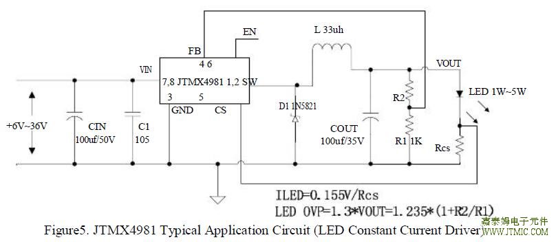
LED Constant Current Driver
四.技术规格书下载(产品PDF)
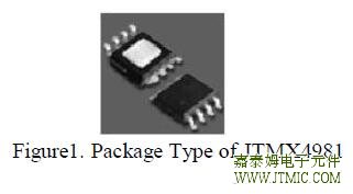
五,产品封装图 (Package)
|
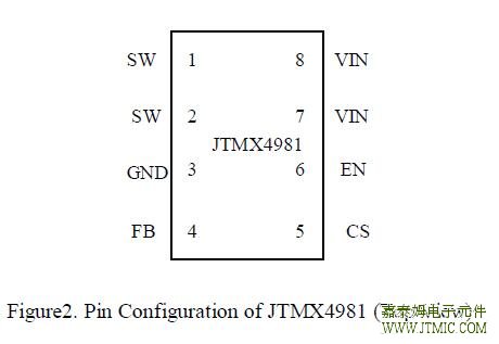
Pin Number |
Pin Name |
Description |
|
1,2 |
SW |
Power Switch Output Pin (SW). Output is the switch node that
supplies power to the output. |
|
3 |
GND |
Ground Pin.(Note: Connected the back exposed PAD to Pin3.) |
|
4 |
FB |
Feedback Pin (FB). Through an external resistor divider
network, Feedback senses the output voltage and regulates it.
The feedback threshold voltage is 1.235V. |
|
5 |
CS |
Output Current Sense Pin; (Iload=0.155V/Rcs) |
|
6 |
EN |
Enable Pin. Drive EN pin low to turn on the device, drive it high
to turn it off. Floating is default low. |
|
7,8 |
VIN |
Supply Voltage Input Pin. JTMX4981 operates from a 4.5V to 40V
DC voltage. Bypass Vin to GND with a suitably large capacitor
to eliminate noise on the input. |
六.电路原理图
七,功能概述
|
Parameter |
Symbol |
Value |
Unit |
|
Input Voltage |
Vin |
-0.3 to 45 |
V |
|
FB Pin Voltage |
VFB |
-0.3 to Vin |
V |
|
EN Pin Voltage |
VEN |
-0.3 to Vin |
V |
|
SW Pin Voltage |
VSW |
-0.3 to Vin |
V |
|
Power Dissipation |
PD |
Internally limited |
mW |
Thermal Resistance
(Junction to Ambient, No Heatsink, Free Air) |
RJA |
60 |
ºC/W |
|
Operating Junction Temperature |
TJ |
-40 to 125 |
ºC |
|
Storage Temperature |
TSTG |
-65 to 150 |
ºC |
|
Lead Temperature (Soldering, 10 sec) |
TLEAD |
260 |
ºC |
|
ESD (HBM) |
|
2000 |
V |
八,相关芯片选择指南
|
产品型号 |
输入电压 |
开关电流 |
开关频率 |
恒压设置 |
恒流设置 |
封装类型 |
|
JTMX4981 |
4.5V ~ 40V |
2A |
150KHz |
Adj (1.235V) |
0.155V |
SOP8L-EP |
|
JTMX4983 |
4.5V ~ 40V |
3A |
150KHz |
Adj (1.235V) |
0.155V |
TO263-5L |

|
8V ~ 40V |
3A |
150KHz |
Adj (1.25V) |
0.11V |
SOP8L-EP |
|
JTMX4984 |
8V ~ 40V |
3A |
180KHz |
Adj (1.25V) |
0.11V |
SOP8L-EP |
|
JTMX4985 |
8V ~ 36V |
5A |
150KHz |
Adj (1.25V) |
0.11V |
TO263-5L |
|
JTMX4986 |
8V ~ 36V |
3A |
180KHz |
Adj (1.25V) |
RCS设置 |
SOP8L |
(责任编辑:oumao18) |


 粤ICP备13004986号-3