|
目录
一,产品概述(General Description)

The JTMX4986 is a 180 KHz fixed frequency PWM buck (step-down)
DC/DC converter,capable of driving a 2.5A load with high efficiency, low
ripple and excellent line and load regulation. Requiring a minimum number
of external components, the regulator is simple to use and include internal
frequency compensation and a fixed-frequency oscillator.
The PWM control circuit is able to adjust the duty ratio linearly from 0 to
100%. An over current protection function is built inside When short protection function happens, the operation frequency will be reduced from 180KHz to
48KHz. An internal compensation block is built in to minimize external component count.
二.产品特点(Features)
Wide 8V to 36V Input Voltage Range
Output Adjustable from 1.25V to 32V
Maximum Duty Cycle 100%
Minimum Drop Out 0.3V
Fixed 180KHz Switching Frequency
Maximum 3A Switching Current
Internal Optimize Power MOSFET
High efficiency
Excellent line and load regulation
With output constant current loop
Built in thermal shutdown function
Built in current limit function
Built in output short protection function
Available in SOP8L package
三,应用范围 (Applications)
Car Charger
Battery Charger
LCD Monitor and LCD TV
Portable instrument power supply
Telecom / Networking Equipment
四.技术规格书下载(产品PDF)
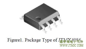
五,产品封装图 (Package)
 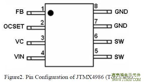
|
Pin Number |
Pin Name |
Description |
|
1 |
FB |
Feedback Pin (FB). Through an external resistor divider
network, FB senses the output voltage and regulates it. The
feedback threshold voltage is 1.25V. |
|
2 |
OCSET |
Output Constant Current Set Pin. |
|
3 |
VC |
Internal Voltage Regulator Bypass Capacity. In typical system
application, The VC pin connect a 1uf capacity to VIN. |
|
4 |
VIN |
Supply Voltage Input Pin. JTMX4986 operates from a 8V to 36V
DC voltage. Bypass Vin to GND with a suitably large
capacitor to eliminate noise on the input. |
|
5,6 |
SW |
Power Switch Output Pin (SW). SW is the switch node that
supplies power to the output. |
|
7,8 |
GND |
Ground Pin. Care must be taken in layout. This pin should be
placed outside of the Schottky Diode to output capacitor
ground path to prevent switching current spikes from inducing
voltage noise into JTMX4986. |
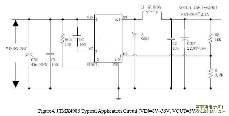
六.电路原理图
七,功能概述
|
Parameter |
Symbol |
Value |
Unit |
|
Input Voltage |
Vin |
-0.3 to 40 |
V |
|
Feedback Pin Voltage |
VFB |
-0.3 to Vin |
V |
|
Output Switch Pin Voltage |
VOutput |
-0.3 to Vin |
V |
|
Power Dissipation |
PD |
Internally limited |
mW |
Thermal Resistance (SOP8L)
(Junction to Ambient, No Heatsink, Free Air) |
RJA |
100 |
ºC/W |
|
Operating Junction Temperature |
TJ |
-40 to 125 |
ºC |
|
Storage Temperature |
TSTG |
-65 to 150 |
ºC |
|
Lead Temperature (Soldering, 10 sec) |
TLEAD |
260 |
ºC |
|
ESD (HBM) |
|
>2000 |
V |
八,相关芯片选择指南
|
产品型号 |
输入电压 |
开关电流 |
开关频率 |
恒压设置 |
恒流设置 |
封装类型 |
|
JTMX4981 |
4.5V ~ 40V |
2A |
150KHz |
Adj (1.235V) |
0.155V |
SOP8L-EP |

|
4.5V ~ 40V |
3A |
150KHz |
Adj (1.235V) |
0.155V |
TO263-5L |
|
JTMX4982 |
8V ~ 40V |
3A |
150KHz |
Adj (1.25V) |
0.11V |
SOP8L-EP |
|
JTMX4984 |
8V ~ 40V |
3A |
180KHz |
Adj (1.25V) |
0.11V |
SOP8L-EP |
|
JTMX4985 |
8V ~ 36V |
5A |
150KHz |
Adj (1.25V) |
0.11V |
TO263-5L |
|
JTMX4986 |
8V ~ 36V |
3A |
180KHz |
Adj (1.25V) |
RCS设置 |
SOP8L |
(责任编辑:oumao18) |


 粤ICP备13004986号-3