 中文
中文 English
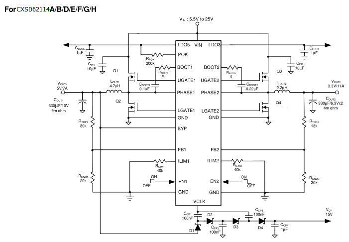
两个低电压降调节器CXSD62114双降压恒定时间同步PWM控制器内部转换MOSFET
| 产品型号: | CXSD62114 |
| 产品类型: | DC-DC转换器 |
| 产品系列: | Buck降压型芯片 |
| 产品状态: | 量产 |
| 浏览次数: | 108 次 |
产品简介
技术参数
| 输入电压范围 (VIN) | 5.5~25V |
|---|---|
| 输出电压 (VOUT) | ADJ |
| 输出电流 (IOUT) | 11 |
| 工作频率 | 1500 |
| 转换效率 | 95% |
| 封装类型 | TQFN3x3-20 |
| Topology | Buck COT降压型芯片 |
| Control method | No. of PWM Outputs:2 |
| Switching frequency | 1500 |
| Protection | Phase: 2 |
| Features | 静态工作电流 Quiescent Current (typ)(uA):280 |
| Application | Bias Voltage (typ) (V):N |
| Operating temp | -40℃~125℃ |
| Reference design | 反馈电压Reference Voltage(V):2 |
产品详细介绍
目录
1.产品概述 2.产品特点
3.应用范围 4.下载产品资料PDF文档
5.产品封装图 6.电路原理图
7.功能概述 8.相关产品
一,产品概述(General Description)
The CXSD62114 integrates dual step-down, constant-on-time,
synchronous PWM controllers (that drives dual N-channel MOSFETs for
each channel) and two low drop-out regulators as well as various protections
into a chip.The PWM controllers step down high voltage of a battery
to generate low-voltage for NB applications. The output of PWM1 and
PWM2 can be adjusted from 2V to 5.5V by setting a resistive voltage-divider
from VOUTx to GND.The linear regulators provide 5V and 3.3V output for
standby power supply. The linear regulators provide up to 100mA output
current. When the PWMx output voltage is higher than LDOx bypass threshold, the related LDOx regulator is shut off and its output is connected to VOUTx
by internal switchover MOSFET. It can save power dissipation. The charge
pump circuit with 250kHz clock driver uses VOUT1 as its power supply to generate ap-proximately 15V DC voltage.
The CXSD62114 provides excellent transient response and accurate DC output voltage in either PFM or PWM Mode. In Pulse-Frequency Mode (PFM),
the CXSD62114 provides very high efficiency over light to heavy loads
with loading-modulated switching frequencies. The Forced-PWM Mode works nearly at constant frequency for low-noise requirements. The unique ultrasonic
mode maintains the switching frequency above 25kHz, which eliminates noise in audio application.The CXSD62114A/D has individual enable controls for
each PWM channels. Pulling both EN1/2 pin low shuts down the all of outputs unless LDO3 output. The LDO3 and LDO5 of CXSD62114B/C are always on standby power.The CXSD62114 is available in a TQFN3x3-20 package.
二.产品特点(Features)
Wide Input voltage Range from 5.5V to 25V
Provide 5 Independent Outputs with ±1.0% Accu-racy Over-Temperature
PWM1 Controller with Adjustable (2V to 5.5V) Out-put
- PWM2 Controller with Adjustable (2V to 5.5V) Out-put
100mA Low Dropout Regulator (LDO5) with Fixed 5V Output
- 100mA Low Dropout Regulator (LDO3) with Fixed 3.3V Output
250kHz Clock Signal for 15V Charge Pump (Used PWM1 as Its Power Supply)
Excellent Line/Load Regulations about±1.5% over
temperature range at PWM Channels
Low Consumption in Standby Mode
2Cells Input Battery Support
Built in POR Control Scheme Implemented
Constant On-Time Control Scheme
Built in Soft Start for PWM Outputs and Soft Stop
for PWM Outputs and LDO Outputs
Integrated Bootstrap Forward P-CH MOSFET
High Efficiency over Light to Full Load Range (PWMs)
Built in Power Good Indicators (PWMs)
60% Under-Voltage and 115% Over-Voltage Protec-tions (PWM)
Adjustable Current-Limit Protection (PWMs)
- Using Sense Low-Side MOSFET’s RDS(ON)
Over-Temperature Protection
3mmx3mm Thin QFN-20 (TQFN3x3-20) package
Lead Free and Green Device Available (RoHS Compliant)
三,应用范围 (Applications)
Notebook and Sub-Notebook Computers
Portable Devices
DDR1, DDR2, and DDR3 Power Supplies
3-Cell and 4-Cell Li+ Battery-Powered Devices
Graphic Cards
Game Consoles
Telecommunications
四.下载产品资料PDF文档
需要详细的PDF规格书请扫一扫微信联系我们,还可以获得免费样品以及技术支持!

五,产品封装图 (Package)


六.电路原理图
七,功能概述
the node.
Decoupling capacitor, the resistor dividers, boot capacitors, and current-limit stetting resistor should
be close to their pins. (For example, place the decoupling ceramic capacitor near the drain of the
high-side MOSFET as close as possible. The bulk capacitors are also placednear the drain).
The input capacitor should be near the drain of the upper MOSFET; the high quality ceramic decoupling
capacitor can be put close to the VCC and GND pins;the output capacitor should be near the loads. The
input capacitor GND should be close to the output ca-pacitor GND and the lower MOSFET GND.
The drain of the MOSFETs (V IN and PHASEx nodes)should be a large plane for heat sinking. And PHASEx
pin traces are also the return path for UGATEx. Con-nect these pins to the respective converter’s upper
MOSFET source.
The controller used ripple mode control. Build the re-sistor divider close to the FB1 pin so that the high
impedance trace is shorter when the output voltage is in ad justable mode. And the FB1 pin traces can’t be
close to the switching signal traces (UGATEx, LGATEx,BOOTx, and PHASEx).
The PGND trace should be a separate trace, and in-dependently go to the source of the low-side MOSFETs
for current-limit accuracy.
八,相关产品 更多同类产品......
|
Switching Regulator > Buck Controller |
||||||||||
|
Part_No |
Package |
Archi tectu |
Phase |
No.of PWM Output |
Output Current (A) |
Input Voltage (V) |
Reference Voltage (V) |
Bias Voltage (V) |
Quiescent Current (uA) |
|
|
min |
max |
|||||||||
|
SOP-14 QSOP-16 QFN4x4-16 |
VM |
1 |
1 |
30 |
2.9 |
13.2 |
0.9 |
12 |
8000 |
|
|
SOP-8 |
VM |
1 |
1 |
20 |
2.9 |
13.2 |
0.8 |
12 |
5000 |
|
|
SOP-8 |
VM |
1 |
1 |
20 |
2.9 |
13.2 |
0.8 |
12 |
5000 |
|
|
QFN4x4-24 |
VM |
2 |
1 |
60 |
3.1 |
13.2 |
0.6 |
12 |
5000 |
|
|
SOP-8 |
VM |
1 |
1 |
20 |
2.2 |
13.2 |
0.8 |
5~12 |
2100 |
|
|
SOP-8 |
VM |
1 |
1 |
20 |
2.2 |
13.2 |
0.8 |
5~12 |
2100 |
|
|
SOP8|TSSOP8 |
VM |
1 |
1 |
5 |
5 |
13.2 |
1.25|0.8 |
5~12 |
3000 |
|
|
SOP-8 |
VM |
1 |
1 |
10 |
3.3 |
5.5 |
0.8 |
5 |
2100 |
|
|
SOP-14 |
VM |
1 |
1 |
10 |
5 |
13.2 |
0.8 |
12 |
2000 |
|
|
TSSOP-24 |QFN5x5-32 |
VM |
1 |
2 |
20 |
5 |
13.2 |
0.6 |
5~12 |
4000 |
|
|
SOP14 QSOP16 QFN-16 |
VM |
1 |
1 |
30 |
2.9 |
13.2 |
0.9 |
12 |
4000 |
|
|
SOP-14 |
VM |
1 |
1 |
30 |
2.2 |
13.2 |
0.6 |
12 |
5000 |
|
|
SOP-14 |
VM |
1 |
1 |
30 |
2.2 |
13.2 |
0.6 |
12 |
5000 |
|
|
SOP-14 |
VM |
1 |
1 |
25 |
2.2 |
13.2 |
0.8 |
12 |
5000 |
|
|
LQFP7x7 48 TQFN7x7-48 |
VM |
1 |
6 |
0.015 |
1.4 |
6.5 |
- |
5 |
1800 |
|
|
TSSOP-24P |
VM |
1 |
2 |
20 |
2.97 |
5.5 |
0.8 |
5~12 |
5000 |
|
|
SOP-14 |
VM |
1 |
1 |
10 |
5 |
13.2 |
0.8 |
12 |
3000 |
|
|
SOP-8-P|DIP-8 |
VM |
1 |
1 |
30 |
2.9 |
13.2 |
1.2 |
12 |
3000 |
|
|
SSOP28 QFN4x4-24 |
VM |
1 |
2 |
20 |
5 |
24 |
0.9 |
5 |
1200 |
|
|
SOP-20 |
VM |
1 |
2 |
20 |
2.2 |
13.2 |
0.6 |
5~12 |
4000 |
|
|
SOP8|DFN3x3-10 |
VM |
1 |
2 |
- |
- |
- |
- |
5~12 |
550 |
|
|
DIP8|SOP-8 |
VM |
1 |
1 |
1 |
1.2 |
9 |
24 |
5 |
9 ~ 24 |
|
|
SSOP16 QFN4x4-16 TQFN3x3-16 |
VM |
1 |
1 |
25 |
3 |
25 |
0.6 |
5 |
1700 |
|
|
TDFN3x3-10 |
COT |
1 |
1 |
25 |
3 |
25 |
0.5 |
5 |
350 |
|
|
QFN4x4-24 |
CM |
2 |
1 |
40 |
4.5 |
13.2 |
0.6 |
5~12 |
4000 |
|
|
SOP8P TDFN3x3-10 |
VM |
1 |
1 |
20 |
3 |
13.2 |
0.8 |
5~12 |
2500 |
|
|
SOP8P |
VM |
1 |
1 |
25 |
3 |
13.2 |
0.6|0.8 |
5~12 |
1200 |
|
|
TDFN3x3-10 |
VM |
1 |
1 |
25 |
4 |
13.2 |
0.8 |
5~12 |
2000 |
|
|
TDFN3x3-10 |
COT |
1 |
1 |
25 |
4.5 |
25 |
0.6 |
5~12 |
80 |
|
|
SOP-8P |
VM |
1 |
1 |
25 |
4.5 |
13.2 |
0.8 |
5~12 |
16000 |
|
|
TQFN3x3-10 |
VM |
1 |
1 |
25 |
4.5 |
13.2 |
0.6 |
5~12 |
2500 |
|
|
TDFN3x3-10 |
COT |
1 |
1 |
30 |
3 |
25 |
0.8 |
5~12 |
2000 |
|
|
TQFN3x3-16 |
COT |
1 |
1 |
30 |
1.8 |
28 |
0.6 |
5 |
600 |
|
|
TQFN 3x3 16 |
COT |
1 |
1 |
30 |
1.8 |
28 |
0.6 |
5 |
600 |
|
|
QFN4x4-24 |
VM |
2 |
1 |
50 |
4.5 |
13.2 |
0.6 |
5~12 |
5000 |
|
|
TQFN4x4-24 |
COT |
1 |
2 |
15 |
6 |
25 |
2 |
N |
550 |
|
|
TQFN4x4-24 |
COT |
1 |
2 |
15 |
6 |
25 |
2 |
N |
550 |
|
|
TQFN4x4-4 TQFN3x3-20 |
COT |
1 |
2 |
20 |
3 |
28 |
0.75 |
5 |
800 |
|
|
TQFN3x3-16 |
COT |
1 |
1 |
20 |
1.8 |
28 |
0.75 |
5 |
400 |
|
|
QFN3.5x3.5-14 TQFN3x3-16 |
COT |
1 |
1 |
20 |
1.8 |
28 |
0.75 |
5 |
400 |
|
|
TQFN3x3-16 |
COT |
1 |
2 |
20 |
1.8 |
28 |
0.75 |
5 |
400 |
|
|
QFN3x3-20 TQFN3x3-16 |
COT |
1 |
2 |
20 |
3 |
28 |
1.8|1.5|0.5 |
5 |
740 |
|
|
TQFN4x4-24 |QFN3x3-20 |
CM |
1 |
2 |
15 |
5 |
28 |
0.5 |
N |
3000 |
|
|
TDFN3x3-10 |
COT |
1 |
1 |
20 |
1.8 |
28 |
0.5 |
5 |
250 |
|
|
TQFN3x3-20 |
COT |
1 |
2 |
15 |
6 |
25 |
2 |
N |
550 |
|
|
TQFN 3x3 20 |
COT |
2 |
2 |
11 |
6 |
25 |
2 |
N |
550 |
|
|
TQFN3x3-20 |
COT |
2 |
2 |
11 |
5.5 |
25 |
2 |
N |
280 |
|
|
QFN4x4-24 |
VM |
2 |
1 |
60 |
3.1 |
13.2 |
0.85 |
12 |
5000 |
|
|
SOP-8P |
VM |
1 |
1 |
20 |
2.9 |
13.2 |
0.8 |
12 |
16000 |
|
|
SOP-20 |
VM |
2 |
2 |
30 |
10 |
13.2 |
1 |
12 |
5000 |
|
|
TDFN3x3-10 |
COT |
1 |
1 |
25 |
1.8 |
28 |
0.7 |
5 |
250 |
|
|
TQFN3x3-20 |
COT |
2 |
1 |
40 |
1.8 |
25 |
REFIN Setting |
5 |
700 |
|
|
QFN 3x3 20 TQFN 3x3 16 |
COT |
1 |
2 |
20 |
3 |
28 |
1.8|1.5 1.35|1.2 0.5 |
5 |
800 |
|
|
TQFN3x3 20 |
COT |
1 |
2 |
15 |
3 |
28 |
0.75 |
5 |
220 |
|
|
TQFN3x3 20 |
COT |
1 |
2 |
15 |
3 |
28 |
0.75 |
5 |
220 |
|
|
TQFN3x3-20 |
COT |
1 |
2 |
20 |
3 |
28 |
0.75 |
5 |
180 |
|

用户评论