 中文
中文 English
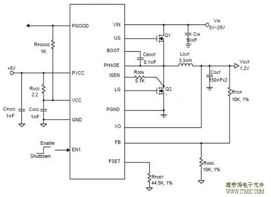
CXSD6292单相恒定时间和同步PWM控制器驱动N通道mosfet降低电池的高压低压芯片
| 产品型号: | CXSD6292 |
| 产品类型: | DC-DC转换器 |
| 产品系列: | Buck降压型芯片 |
| 产品状态: | 量产 |
| 浏览次数: | 101 次 |
产品简介
技术参数
| 输入电压范围 (VIN) | 3~25V |
|---|---|
| 输出电压 (VOUT) | ADJ |
| 输出电流 (IOUT) | 25 |
| 工作频率 | 1500 |
| 转换效率 | 95% |
| 封装类型 | SSOP-16|QFN4x4-16|TQFN3x3-16 |
| Features | 静态工作电流 Quiescent Current (typ)(uA):1700 |
| Topology | Buck VM降压型芯片 |
| Protection | Phase: 1 |
| Application | Bias Voltage (typ) (V):5 |
| Control method | No. of PWM Outputs:1 |
| Operating temp | -40℃~125℃ |
| Reference design | 反馈电压Reference Voltage(V):0.6 |
| Switching frequency | 1500 |
产品详细介绍
目录
1.产品概述 2.产品特点
3.应用范围 4.下载产品资料PDF文档
5.产品封装图 6.电路原理图
7.功能概述 8.相关产品
一,产品概述(General Description)
The CXSD6292 is a single-phase, constant-on-time, and synchronous
PWM controller which drives N-channel MOSFETs. The CXSD6292 steps
down high voltage of a battery to generate low-voltage chipset or RAM supplies
in notebook computers.
The CXSD6292 provides excellent transient response and accurate DC
voltage output in either PFM or PWM Mode.In Pulse Frequency Modulation
(PFM) Mode, the CXSD6292 provides very high efficiency over light load
with loading-modulated switching frequencies. When the inductor current
is continuous, the operation automatically enters PWM mode with relatively
constant switching frequency.For QFN4x4-16A and TQFN3x3-16 packages,
the Forced-PWM Mode works nearly at constant frequency for low-noise
requirements.
The CXSD6292 is equipped with accurate over-current,output under-
voltage, and over-voltage protections per-fect for NB application. A Power-
On-Reset function moni-tors the voltage on VCC pin to prevent errorneous
opera-tion during power-on. The CXSD6292 has a digital soft-start and soft-stop.
The internal integrated soft-start ramps up the output voltage with controlled slew
rate to reduce the start-up current. The digital soft-stop function actively discharges
the output capacitors with controlled reverse inductor current.
The CXSD6292 is available in SSOP-16, QFN4x4-16A, and TQFN3x3-16 packages
二.产品特点(Features)
1.)Adjustable Output Voltage from +0.6V to +3.3V
- 0.6V Reference Voltage
- ±1% Accuracy Over Temperature
2.)Operates from an Input Battery Voltage Range of +3V to +25V
3.)Wide Output Load Range from 0A to 25A
4.)Power-On-Reset Monitoring on VCC Pin
5.)Excellent Line and Load Transient Response
6.)PFM Mode for Increased Light Load Efficiency
7.)Programmable PWM Frequency from 200kHz to 600kHz
8.)Integrated MOSFET Drivers and Bootstrap Diode
9.)Internal Integrated Soft-Start and Soft-Stop
10.)Selectable Forced PWM or Automatic PFM/PWM
11.)Mode (only for QFN4x4-16A and TQFN3x3-16 Packages)
Power Good Monitoring
12.)Fault Identification by PGOOD Pull-Down Resistance
13.)70% Under-Voltage Protection (UVP)
14.)124% Over-Voltage Protection (OVP)
15.)Adjustable Over-Current Protection (OCP)
- Sensing Low-Side MOSFET’s Current
16.)Over-Temperature Protection (OTP)
17.)SSOP-16, Compact 4mmx4mm QFN-16 (QFN4x4-
16A), and TQFN3x3-16 Packages
18.)Lead Free and Green Devices Available
三,应用范围 (Applications)
PCI Express Graphical Processing Unit
Notebook Adapter
Auxiliary Power Rail
VRM
四.下载产品资料PDF文档
需要详细的PDF规格书请扫一扫微信联系我们,还可以获得免费样品以及技术支持!

五,产品封装图 (Package)


六.电路原理图
七,功能概述
Power Good Indicator
The CXSD6292 features an open-drain PGOOD output pin to indicate one of the IC’s working statuses
including soft-start, under-voltage fault, over-current fault, and over-voltage faule. The unique fault-
identification capability can drastically reduce trouble-shooting time and effort.
The pull-down resistance of the PGOOD pin correspondsto the fault status of the controller. During
soft-start or if an under voltage fault occurs, the PGOOD pull-down re-sistance is 95Ω, or 32Ω for
an over current fault, or 63Ω for an over voltage fault. The pull-low resistance is unde-fined if VCC
is below the rising/falling POR threshold.
Over-Temperature Protection (OTP)
When the junction temperature increases above the ris-ing threshold temperature TOTR, the IC
will enter the over-temperature protection (OTP) state that suspends the PWM, which forces the
LG and UG gate drivers to output low voltages. The status of the PGOOD pin does not change, nor
does the converter latch-off. The thermal sensor allows the converters to start a start-up process
and regulate the output voltage again after the junction temperature cools by 25oC. The OTP is
designed with a 25oC hysteresis to lower the average TJ during continu-ous thermal overload
conditions, which increases life- time of the CXSD6292.
Over-Current Protection (OCP) and Short-Circuit Pro-tection (SCP)
The over-current protection (OCP) is designed to resist the slow slew rate load current; on the other
hand, the short-circuit protection (SCP) is used to take care of rapid shorted output. The setpoint for
OCP and SCP is pro-grammed with resistor RSEN that is connected across the ISEN pin and drain of
the low-side MOSFET. The SCP setpoint is internally set to twice the OCP setpoint.
The inductor current develops a negative voltage across the RDS(ON) of the low-side MOSFET that is
sampled and held shortly before LG gate-driver output goes low. The OCP fault occurs if ISEN rises
above the OCP threshold current IOC (typical :26μA) while attempting to null the nega-tive voltage
across the PHASE and GND pins. When the ISEN exceeds IOC, the OCP counter starts to work.
Meanwhile, pulses on all the PWM (ISEN > IOC) remains for 20μs, the OCP will be triggered. When
ISEN falls below IOC on a PWM pulses before 20μs has elapsed, the counter will be reset. The SCP
fault will occur within 10μs when I SEN exceeds twice I OC. The relationship between the sampled
current and MOSFET current is given by:
ISEN × RSEN = RDS ( ON ) × IL
Which means the current sensing pin will source current to make the voltage drop on the MOSFET
and is equal to the voltage generated on the sensing resistor along the ISEN pin current flowing path.
八,相关产品 更多同类产品......
|
Switching Regulator > Buck Controller |
||||||||||
|
Part_No |
Package |
Archi tectu |
Phase |
No.of PWM Output |
Output Current (A) |
Input Voltage (V) |
Reference Voltage (V) |
Bias Voltage (V) |
Quiescent Current (uA) |
|
|
min |
max |
|||||||||
|
SOP-14 QSOP-16 QFN4x4-16 |
VM |
1 |
1 |
30 |
2.9 |
13.2 |
0.9 |
12 |
8000 |
|
|
SOP-8 |
VM |
1 |
1 |
20 |
2.9 |
13.2 |
0.8 |
12 |
5000 |
|
|
SOP-8 |
VM |
1 |
1 |
20 |
2.9 |
13.2 |
0.8 |
12 |
5000 |
|
|
QFN4x4-24 |
VM |
2 |
1 |
60 |
3.1 |
13.2 |
0.6 |
12 |
5000 |
|
|
SOP-8 |
VM |
1 |
1 |
20 |
2.2 |
13.2 |
0.8 |
5~12 |
2100 |
|
|
SOP-8 |
VM |
1 |
1 |
20 |
2.2 |
13.2 |
0.8 |
5~12 |
2100 |
|
|
SOP8|TSSOP8 |
VM |
1 |
1 |
5 |
5 |
13.2 |
1.25|0.8 |
5~12 |
3000 |
|
|
SOP-8 |
VM |
1 |
1 |
10 |
3.3 |
5.5 |
0.8 |
5 |
2100 |
|
|
SOP-14 |
VM |
1 |
1 |
10 |
5 |
13.2 |
0.8 |
12 |
2000 |
|
|
TSSOP-24 |QFN5x5-32 |
VM |
1 |
2 |
20 |
5 |
13.2 |
0.6 |
5~12 |
4000 |
|
|
SOP14 QSOP16 QFN-16 |
VM |
1 |
1 |
30 |
2.9 |
13.2 |
0.9 |
12 |
4000 |
|
|
SOP-14 |
VM |
1 |
1 |
30 |
2.2 |
13.2 |
0.6 |
12 |
5000 |
|
|
SOP-14 |
VM |
1 |
1 |
30 |
2.2 |
13.2 |
0.6 |
12 |
5000 |
|
|
SOP-14 |
VM |
1 |
1 |
25 |
2.2 |
13.2 |
0.8 |
12 |
5000 |
|
|
LQFP7x7 48 TQFN7x7-48 |
VM |
1 |
6 |
0.015 |
1.4 |
6.5 |
- |
5 |
1800 |
|
|
TSSOP-24P |
VM |
1 |
2 |
20 |
2.97 |
5.5 |
0.8 |
5~12 |
5000 |
|
|
SOP-14 |
VM |
1 |
1 |
10 |
5 |
13.2 |
0.8 |
12 |
3000 |
|
|
SOP-8-P|DIP-8 |
VM |
1 |
1 |
30 |
2.9 |
13.2 |
1.2 |
12 |
3000 |
|
|
SSOP28 QFN4x4-24 |
VM |
1 |
2 |
20 |
5 |
24 |
0.9 |
5 |
1200 |
|
|
SOP-20 |
VM |
1 |
2 |
20 |
2.2 |
13.2 |
0.6 |
5~12 |
4000 |
|
|
SOP8|DFN3x3-10 |
VM |
1 |
2 |
- |
- |
- |
- |
5~12 |
550 |
|
|
DIP8|SOP-8 |
VM |
1 |
1 |
1 |
1.2 |
9 |
24 |
5 |
9 ~ 24 |
|
|
SSOP16 QFN4x4-16 TQFN3x3-16 |
VM |
1 |
1 |
25 |
3 |
25 |
0.6 |
5 |
1700 |
|
|
TDFN3x3-10 |
COT |
1 |
1 |
25 |
3 |
25 |
0.5 |
5 |
350 |
|
|
QFN4x4-24 |
CM |
2 |
1 |
40 |
4.5 |
13.2 |
0.6 |
5~12 |
4000 |
|
|
SOP8P TDFN3x3-10 |
VM |
1 |
1 |
20 |
3 |
13.2 |
0.8 |
5~12 |
2500 |
|
|
SOP8P |
VM |
1 |
1 |
25 |
3 |
13.2 |
0.6|0.8 |
5~12 |
1200 |
|
|
TDFN3x3-10 |
VM |
1 |
1 |
25 |
4 |
13.2 |
0.8 |
5~12 |
2000 |
|
|
TDFN3x3-10 |
COT |
1 |
1 |
25 |
4.5 |
25 |
0.6 |
5~12 |
80 |
|
|
SOP-8P |
VM |
1 |
1 |
25 |
4.5 |
13.2 |
0.8 |
5~12 |
16000 |
|
|
TQFN3x3-10 |
VM |
1 |
1 |
25 |
4.5 |
13.2 |
0.6 |
5~12 |
2500 |
|
|
TDFN3x3-10 |
COT |
1 |
1 |
30 |
3 |
25 |
0.8 |
5~12 |
2000 |
|
|
TQFN3x3-16 |
COT |
1 |
1 |
30 |
1.8 |
28 |
0.6 |
5 |
600 |
|
|
TQFN 3x3 16 |
COT |
1 |
1 |
30 |
1.8 |
28 |
0.6 |
5 |
600 |
|
|
QFN4x4-24 |
VM |
2 |
1 |
50 |
4.5 |
13.2 |
0.6 |
5~12 |
5000 |
|
|
TQFN4x4-24 |
COT |
1 |
2 |
15 |
6 |
25 |
2 |
N |
550 |
|
|
TQFN4x4-24 |
COT |
1 |
2 |
15 |
6 |
25 |
2 |
N |
550 |
|
|
TQFN4x4-4 TQFN3x3-20 |
COT |
1 |
2 |
20 |
3 |
28 |
0.75 |
5 |
800 |
|
|
TQFN3x3-16 |
COT |
1 |
1 |
20 |
1.8 |
28 |
0.75 |
5 |
400 |
|
|
QFN3.5x3.5-14 TQFN3x3-16 |
COT |
1 |
1 |
20 |
1.8 |
28 |
0.75 |
5 |
400 |
|
|
TQFN3x3-16 |
COT |
1 |
2 |
20 |
1.8 |
28 |
0.75 |
5 |
400 |
|
|
QFN3x3-20 TQFN3x3-16 |
COT |
1 |
2 |
20 |
3 |
28 |
1.8|1.5|0.5 |
5 |
740 |
|
|
TQFN4x4-24 |QFN3x3-20 |
CM |
1 |
2 |
15 |
5 |
28 |
0.5 |
N |
3000 |
|
|
TDFN3x3-10 |
COT |
1 |
1 |
20 |
1.8 |
28 |
0.5 |
5 |
250 |
|
|
TQFN3x3-20 |
COT |
1 |
2 |
15 |
6 |
25 |
2 |
N |
550 |
|
|
TQFN 3x3 20 |
COT |
2 |
2 |
11 |
6 |
25 |
2 |
N |
550 |
|
|
TQFN3x3-20 |
COT |
2 |
2 |
11 |
5.5 |
25 |
2 |
N |
280 |
|
|
QFN4x4-24 |
VM |
2 |
1 |
60 |
3.1 |
13.2 |
0.85 |
12 |
5000 |
|
|
SOP-8P |
VM |
1 |
1 |
20 |
2.9 |
13.2 |
0.8 |
12 |
16000 |
|
|
SOP-20 |
VM |
2 |
2 |
30 |
10 |
13.2 |
1 |
12 |
5000 |
|
|
TDFN3x3-10 |
COT |
1 |
1 |
25 |
1.8 |
28 |
0.7 |
5 |
250 |
|
|
TQFN3x3-20 |
COT |
2 |
1 |
40 |
1.8 |
25 |
REFIN Setting |
5 |
700 |
|
|
QFN 3x3 20 TQFN 3x3 16 |
COT |
1 |
2 |
20 |
3 |
28 |
1.8|1.5 1.35|1.2 0.5 |
5 |
800 |
|
|
TQFN3x3 20 |
COT |
1 |
2 |
15 |
3 |
28 |
0.75 |
5 |
220 |
|
|
TQFN3x3 20 |
COT |
1 |
2 |
15 |
3 |
28 |
0.75 |
5 |
220 |
|
|
TQFN3x3-20 |
COT |
1 |
2 |
20 |
3 |
28 |
0.75 |
5 |
180 |
|

用户评论