|
目录
一,产品概述(General Description) The JTMX4003 JTMX4005 is a 300KHz fixed frequency PWM buck (step-down)DC/DC converter,capable of driving a 4A load with high efficiency, low ripple and excellent line and load regulation.Requiring a minimum number of external components, the regulator is simple to use and include internal frequency compensation and a fixed-frequency oscillator. The PWM control circuit is able to adjust the duty ratio linearly from 0 to 100%. An enable function, an over current protection function is built inside. When short protection function happens, the operation frequency will be reduced from 300KHz to 60KHz. An internal compensation block is built in to minimize external component count. 二.产品特点(Features) Wide 5V to 32V Input Voltage Range Output Adjustable from 0.8V to 30V Maximum Duty Cycle 100% Minimum Drop Out 0.6V Fixed 300KHz Switching Frequency 4A Constant Output Current Capability Internal Optimize Power MOSFET High efficiency Excellent line and load regulation TTL shutdown capability EN pin with hysteresis function Built in thermal shutdown function Built in current limit function Built in output short protection function Available in TO-252 package 三,应用范围 (Applications)
LCD Monitor and LCD TV
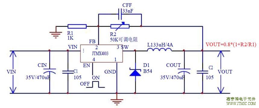 七.JTMX4003 DEMO BOARD MANUAL (一)JTMX4003 12V 转 5V 应用电路测试数据: 1. JTMX4003 12V 转 5V(负载 0.5A~4A)应用电路图:  2. JTMX4003 12V 转 5V(负载 0.5A~4A)测试数据及效率图:
 (二)JTMX4003 24V 转 12V 应用电路测试数据: 1.JTMX4003 24V 转 12V(负载 0.5A~4A)应用电路图: 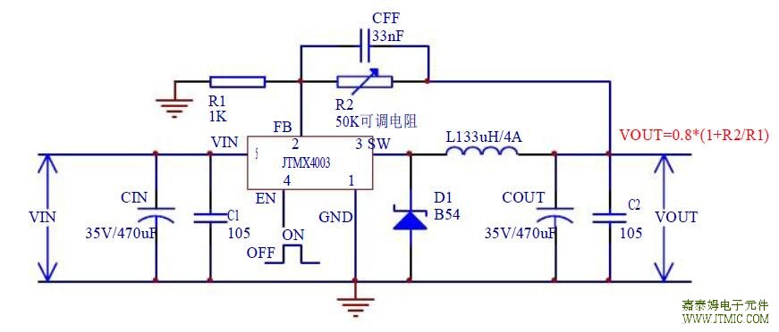 2. JTMX4003 24V 转 12V(负载 0.5A~4A)测试数据及效率:
 (三)JTMX4003 PCB 板布局建议: (1)流大电流的线要粗,短,不拐弯。 (2)1 脚(GND),5 脚(VIN)线要粗,短线,不拐弯,且输入电解电容 CIN 和 105 C1 陶瓷电容紧挨第 5 脚 (VIN)和 1 脚(GND)。(主要是为了减小输入电源布线寄生的电感,电阻产生的高压开关毛刺干扰) (3)3 脚(SW)输出线要粗,短线,不拐弯,电感和续流二极管要紧挨第 3 脚(SW)输出端。 (4)2 脚(FB)走线要接到输出滤波电容 C2,COUT 之后, PCB 布线远离 L1,D1,避免噪声干扰。 (5)增加 PCB 板铜薄的厚度。(DEMO 板用 130um 厚铜薄双面 PCB 板材料) (6)适当的增加 JTMX4003 芯片衬底与 PCB 板的接触面积,提高芯片散热能力,注意 JTMX4003 芯片衬底是 SW 端。 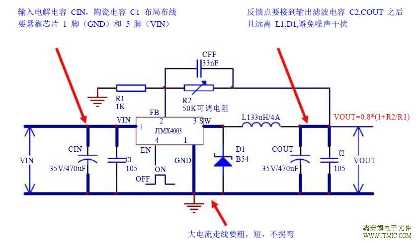 JTMX4003PCB 图: 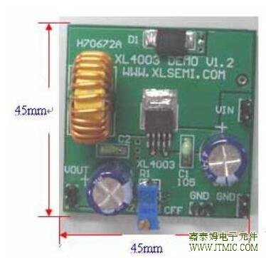 (四)JTMX4003 温度测试数据 1:JTMX4003 电路图和 PCB 图: 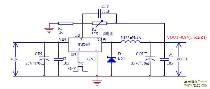 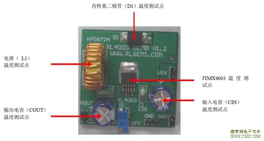 2:JTMX4003 DEMO 板工作时(12V 转 5V)各元件温度,自然通风,室温:27℃。 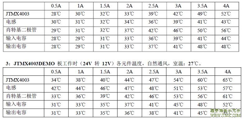
(五)JTMX4003 实现恒流具体方案
1JTMX4003 恒流原理图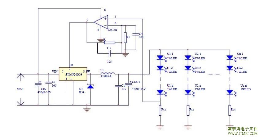 说 明 : 先 把 RCS 的 功 耗 降 下 来 , 把 VRCS 放 大 几 倍 之 后 与 FB 关 联 。 其 中 放 大 器 VAR1=VRCS(1+R6/R5) ,例如设定恒流电路单路 ICS =300mA,RCS=0.33R, 那么 VCS=RCS*ICS 0.099V 由于 VAR1=0.8V 那么放大器调解成放大 8.倍,那么 R5,R6 的值就可以得出来了。 八,功能概述
(责任编辑:oumao18) |


 粤ICP备13004986号-3