


目录
一,产品概述(General Description)
VDSS=40V/VGSS=±20V/ID=130A
RDS(ON)=4mΩ(max.)@VGS=10V
High Dense Cell Design
Reliable and Rugged
Advanced trench process technology
High Density Cell Design For Ultra Low
On-Resistance
四.下载产品资料PDF文档
 |
JTM1404B |
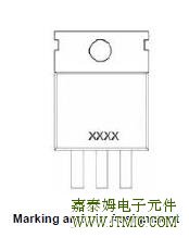
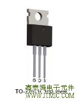
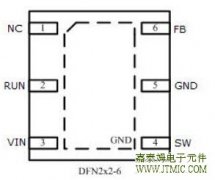
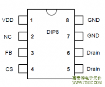
五,产品封装图 (Package)
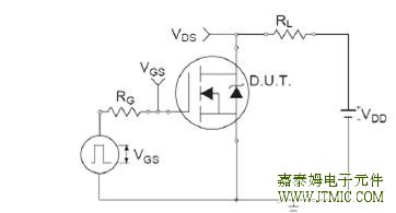
六.电路原理图
七,功能概述
Any and all H&M SEMI products described or contained herein do not have specifications that can handle applications that require extremely high levels of reliability, such as life-support systems, aircraft's control systems, or other applications whose failure can be reasonably expected to result in serious physical and/or material damage. Consult
with your H&M SEMI representative nearest you before using any H&M SEMI products described or contained herein in
such applications.
H&M SEMI assumes no responsibility for equipment failures that result from using products at values
H&M SEMI assumes no responsibility for equipment failures that result from using products at values
that exceed, even momentarily, rated values (such as maximum ratings, operating condition ranges, or other parameters)
listed in products specifications of any and all H&M SEMI products described or contained herein.
Specifications of any and all H&M SEMI products described or contained herein stipulate the performance, characteristics,and functions of the described products in the independent state, and are not guarantees of the performance, characteristics,and functions of the described products as mounted in the customer’s products or equipment. To verify symptoms and states that cannot be evaluated in an independent device, the customer should
always evaluate and test
devices mounted in the customer’s products or equipment.always evaluate and test
Jiataimu CO.,LTD. strives to supply high-quality high-reliability products. However, any and all
semiconductor products fail with some probability. It is possible that these probabilistic failures could
give rise to accidents or events that could endanger human lives, that could give rise to smoke or fire, or that could
cause damage to other property. When designing equipment, adopt safety measures so that these kinds of accidents or
events cannot occur. Such measures include but are not limited to protective circuits and error prevention circuits for safe
design, redundant design, and structural design.cause damage to other property. When designing equipment, adopt safety measures so that these kinds of accidents or
events cannot occur. Such measures include but are not limited to protective circuits and error prevention circuits for safe
In the event that any or all H&M SEMI products(including technical data, services) described or contained herein are
controlled under any of applicable local export control laws and regulations, such products must not be exported without
obtaining the export license from the authorities concerned in accordance with the above law.
No part of this publication may be reproduced or transmitted in any form or by any means, electronic or mechanical, including photocopying and recording, or any information storage or retrieval system, or otherwise, without the prior written permission of Jiataimu CO.,LTD.Information (including circuit diagrams and circuit parameters) herein is for example only ; it is not guaranteed for volume production. H&M SEMI believes information herein is accurate and reliable, but no guarantees are made or implied regarding its use or any infringements of intellectual property rights or other rights of third parties.Any and all information described or contained herein are subject to change without notice due to product/technology improvement, etc. When designing equipment, refer to the "Delivery Specification" for the
product that you intend to use.This catalog provides information as of Sep.2010. Specifications and information herein are subject to change without notice.
八,相关产品
| 备注: | ||||||||||
| 1. 标注的Id电流是MOS芯片的最大常态电流,实际使用时的最大常态电流还要受封装的最大电流限制。因此客户设计产品时的最大使用电流设定要考虑封装的最大电流限制。建议客户设计产品时的最大使用电流设定更重要的是要考虑MOS的内阻参数。 | ||||||||||
| 2. 建议在MOS的栅源(G/S)极之间并一个电阻(10K)和一个稳压二极管(5V-12V)起到保护栅源(G/S)极过压的作用。 | ||||||||||
| 3.建议MOS管的开启电压尽量提高,这样MOS管才能充分开启导通,这个时候内阻最小,不容易发烫。一般建议低压MOS的VGS开启电压设定为4.5V以上,中高压MOS的开启电压设定为10V以上. | ||||||||||
| 4.MOS 电路操作注意事项: | ||||||||||
| 静电在很多地方都会产生,采取下面的预防措施,可以有效防止MOS 电路由于受静电放电影响而引起的损坏: | ||||||||||
| • 操作人员要通过防静电腕带接地。 | ||||||||||
| • 设备外壳必须接地。 | ||||||||||
| • 装配过程中使用的工具必须接地。 | ||||||||||
| • 必须采用导体包装或抗静电材料包装或运输 | ||||||||||
| 我司的JTM2301/SOT-23/3A/20V/PMOS的优点:是足3A的电流,内阻小,和市场低端的1A的产品不同,可以用于移动电源/充电器/多节保护板/家电/航模/遥控玩具等大电流/低内阻的应用场合。 | ||||||||||
| 我司的JTM2302/SOT-23/3A/20V/NMOS的优点:是足3A的电流,内阻小,和市场低端的1A的产品不同,可以用于移动电源/充电器/多节保护板/家电/航模/遥控玩具等大电流/低内阻的应用场合。 | ||||||||||
| 我司的JTM3400/SOT-23-3L/5.8A/30V/NMOS的优点:是足5.8A的电流/大SOT-23封装的,内阻小,和市场低端的小SOT-23的不同,可以用于移动电源/充电器/多节保护板/家电/航模/遥控玩具等大电流/低内阻的应用场合。 | ||||||||||
| 我司的JTM3401/SOT-23-3L/4.2A/30V/PMOS的优点:是足4.2A的电流/大SOT-23封装的,内阻小,和市场低端的小SOT-23的不同,可以用于移动电源/充电器/多节保护板/家电/航模/遥控玩具等大电流/低内阻的应用场合。 | ||||||||||
| 我司的JTM2310/SOT-23-3L/3A/60V/NMOS的优点:1.耐压可达60V,足3A电流,大SOT-23封装的。2.可以用于LED照明等耐压高的产品应用。 | ||||||||||
| 我司的JTM4953的优点:电流大内阻小,可以用于全彩屏市场。 | ||||||||||
| 我司的JTM4430的优点:电流大内阻小,电流可达18A.目前市场上SOP8/NMOS电流最大的一款产品之一。 | ||||||||||
| 我司的JTM4440的优点:耐压可达60V, 目前市场上SOP8/NMOS耐压最大的一款产品之一。 | ||||||||||
| JTM8810E/SOT-26&TSSOP8/7A/20V/双NMOS的优点:足7A的电流,带ESD静电保护,相比市场上的8205,电流更大内阻更小,可直接替换AO8810/AO8820/AO8822/SSF2418E/SSF2816E,主要可用于高端的锂电保护板/手机电池/多节保护板/移动电源/充电器/家电/航模/遥控玩具等大电流/低内阻的应用场合。 | ||||||||||
| 产品应用: | ||||||||||
| 1.MP3/MP4/MP5/PMP 播放器 | ||||||||||
| 2.MID/UMPC | ||||||||||
| 3.GPS/蓝牙耳机 | ||||||||||
| 4.PDVD/车载DVD/汽车音响 | ||||||||||
| 5.液晶电视/液晶显示器 | ||||||||||
| 6.移动电源/电子烟 | ||||||||||
| 7.手机电池、锂电池保护板 | ||||||||||
| 8.LED照明/LED电源 | ||||||||||
| 9.LED显示屏 | ||||||||||
| 10.智能充电器 | ||||||||||
| 11.小家电、家电控制板 | ||||||||||
| 12.电脑主板、显卡 | ||||||||||
 Allegro 的 ACS726 电流传感器
人气:216
Allegro 的 ACS726 电流传感器
人气:216
 The JTM3410D is a constant freq
人气:195
The JTM3410D is a constant freq
人气:195
 SFL710是针对Buck架构优化的
人气:193
SFL710是针对Buck架构优化的
人气:193
 NUP45V6、NUP46V8和NUP412V全球
人气:183
NUP45V6、NUP46V8和NUP412V全球
人气:183
 内置高低压过流补偿实现
人气:182
内置高低压过流补偿实现
人气:182
 双通道AAT1270采用一个带小
人气:163
双通道AAT1270采用一个带小
人气:163
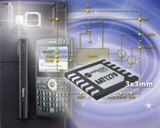
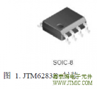 JTM6283B是一款升压恒流型
人气:160
JTM6283B是一款升压恒流型
人气:160
 ADF5904 接收器降频转换器
人气:158
ADF5904 接收器降频转换器
人气:158
 JM100支持 QC2.0 协议的低成
人气:132
JM100支持 QC2.0 协议的低成
人气:132
 自动补偿输入电压,电感
人气:131
自动补偿输入电压,电感
人气:131
 粤ICP备13004986号-3