

1.产品概述 2.产品特点
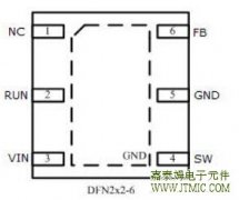
3.应用范围 4.产品封装图
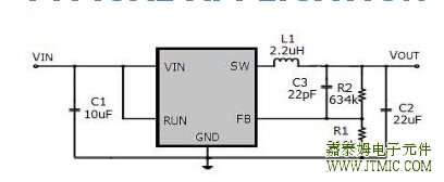
5.电路原理图 6.产品PCB
7.产品BOM 8.产品PDF文档
9.功能概述
一,产品概述(General Description)
The JTM3410D is a constant frequency, current mode step-down converter. The device integrates a main switch and a synchronous rectifier for high efficiency
without an external Schottky diode. It is ideal for portable equipment requiring very high current up to 1.3A from single-cell Lithium-ion batteries while still achieving over 96% efficiency during peak load conditions. The JTM3410D also can run at 100% duty cycle for low dropout operation, extending battery life in portable systems while light load operation provides very low output ripple for noise sensitive applications.
This device offers two operation modes, PWM control and PFM Mode switching control, which allows a high efficiency over the wider range of the
load.
二.产品特点(Features)
1.High Efficiency: Up to 96%
2.1.5MHz Constant Frequency Operation
3.1.3A Output Current
4.No Schottky Diode Required
5.2.3V to 6V Input Voltage Range
6.Output Voltages from 0.6V to VIN
7.PFM Mode for High Efficiency in Light Load
8.100% Duty Cycle in Dropout Operation
9Low Quiescent Current: 35µA
10.Slope Compensated Current Mode Control for
11.Excellent Line and Load Transient Response
12.Short Circuit Protection
13.Thermal Fault Protection
14.Inrush Current Limit and Soft Start
15.<1µA Shutdown Current
16.Available IN WDFN22-6L
17.-40°C to +85°C Temperature Range
三,应用范围 (Applications)
1.Cellular and Smart Phones
2.Wireless and DSL Modems PDAs
3.Digital Still and Video Cameras
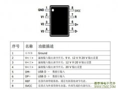
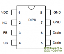
四,产品封装图 (Package)

五,电路原理图
六, 产品PCB
(略)
七.产品BOM
(略)
八.产品PDF文档
 |
JTM3410 |
九,功能概述
The JTM3410D is a hi gh output current monolithic switch mode step-down DC-DC converter. The device operates at a fixed 1.5MHz switching frequency, and uses a slope compensated current mode architecture. This step-down DC-DC converter can supply up to 1.3A output current at VIN = 3V and has an input voltage range from 2.3V to 6V. It minimizes external component size and optimizes efficiency at the heavy load range. The slope compensation allows the device to remain stable over a wider range of inductor values so that smaller values (1μH to 4.7μH) with lower DCR can be used to achieve higher efficiency. Apart from the small bypass input capacitor, only a s mall L-C filter is required at the output.. The adjustable output voltage can be programmed with external feedback to any voltage, ranging from 0.6V to near the input voltage. It uses internal MOSFETs to achieve high efficiency and can generate very low output voltages by using an internal reference of 0.6V. At dropout operation, the converter duty cycle increases to 100% and the output voltage tracks the input voltage minus the low RDS(ON) drop of the P-channel high-side MOSFET and the inductor DCR. The internal error amplifier and compensation provides excellent transient response, load and line regulation.Internal soft start eliminates any output voltage overshoot when the enable or the input voltage is applied.
 Allegro 的 ACS726 电流传感器
人气:216
Allegro 的 ACS726 电流传感器
人气:216
 SFL710是针对Buck架构优化的
人气:193
SFL710是针对Buck架构优化的
人气:193
 NUP45V6、NUP46V8和NUP412V全球
人气:183
NUP45V6、NUP46V8和NUP412V全球
人气:183
 内置高低压过流补偿实现
人气:182
内置高低压过流补偿实现
人气:182
 ADF5904 接收器降频转换器
人气:168
ADF5904 接收器降频转换器
人气:168
 双通道AAT1270采用一个带小
人气:163
双通道AAT1270采用一个带小
人气:163
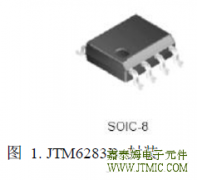 JTM6283B是一款升压恒流型
人气:160
JTM6283B是一款升压恒流型
人气:160
 JM100支持 QC2.0 协议的低成
人气:132
JM100支持 QC2.0 协议的低成
人气:132
 自动补偿输入电压,电感
人气:131
自动补偿输入电压,电感
人气:131
 粤ICP备13004986号-3