|
目录
一,产品概述(General Description) The JTMX6007 JTMX6008regulator is a wide input range,current mode, DC/DC converter which is capable of generating either positive or negative output voltages. It can be configured as either a boost, flyback, SEPIC or inverting converter. The JTMX6007 built in N-channel power MOSFET and fixed frequency oscillator, current-mode architecture results in stable operation over a wide range of supply and output voltages. The JTMX6007 JTMX6008 regulator is special design for portable electronic equipment. 二.产品特点(Features) Wide 3.6V to 24V Input Voltage Range Positive or Negative Output Voltage Programming with a Single Feedback Pin Current Mode Control Provides Excellent Transient Response 1.25V reference adjustable version Fixed 400KHz Switching Frequency Maximum 2A Switching Current SW PIN Built in Over Voltage Protection Excellent line and load regulation EN PIN TTL shutdown capability Internal Optimize Power MOSFET High efficiency up to 90% Built in Frequency Compensation Built in Soft-Start Function Built in Thermal Shutdown Function Built in Current Limit Function Available in SOP8L package 三,应用范围 (Applications)
Automotive and Industrial Boost
Portable Electronic EquipmentBuck-Boost / Inverting Converters 四.技术规格书下载(产品PDF)
 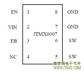
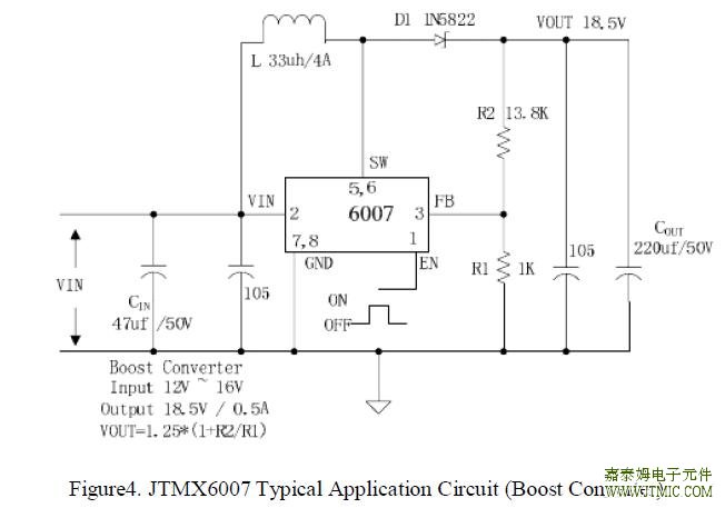 七,功能概述
(责任编辑:oumao18) |


 粤ICP备13004986号-3