


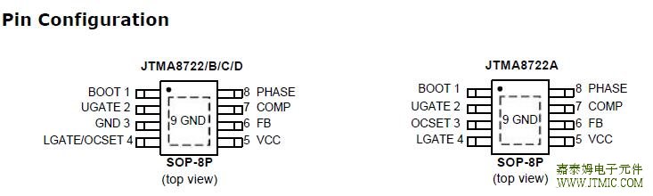
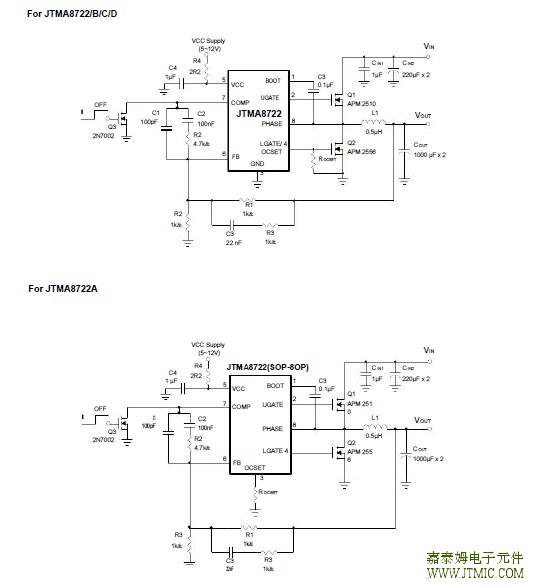
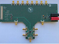
六.电路原理图
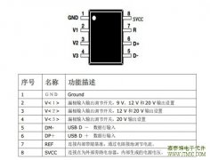
七,功能概述
Layout Consideration
In any high switching frequency converter, a correct lay-out is important to ensure proper operation of theregulator. With power devices switching at 300kHz,the resulting current transient will cause voltage spike
across the interconnecting impedance and parasitic circuit elements. As an example, consider the turn-off
transition of the PWM MOSFET. Before turn-off, the MOSFET is car-rying the full load current. During turn-off,
current stops flowing in the MOSFET and is free-wheeling by the lower MOSFET and parasitic diode. Any
parasitic inductance of the circuit generates a large voltage spike during the switching interval. In general,
using short and wide printed circuit traces should minimize interconnecting imped ances and the magnitude
of voltage spike. And signal and power grounds are to be kept separate till combined using ground plane
construction or single point grounding. Figure 8. illustrates the layout, with bold lines indicating high current
paths; these traces must be short and wide. Components along the bold lines should be placed lose together.
Below is a checklist for your layout:
- Keep the switching nodes (UGATE, LGATE, and PHASE)away from sensitive small signal nodes since these
nodes are fast moving signals. Therefore, keep traces to these nodes as short as possible.
- The traces from the gate drivers to the MOSFETs (UGand LG) should be short and wide.
- Place the source of the high-side MOSFET and the drain of the low-side MOSFET as close as possible. Minimiz-
ing the impedance with wide layout plane between the two pads reduces the voltage bounce of the node.
- Decoupling capacitor, compensation component, the resistor dividers, and boot capacitors should be close
their pins. (For example, place the decoupling ceramic capacitor near the drain of the high-side MOSFET as
close as possible. The bulk capacitors are also placed near the drain).
- The input capacitor should be near the drain of the up-per MOSFET; the output capacitor should be near the
loads. The input capacitor GND should be close to the output capacitor GND and the lower MOSFET GND.
The drain of the MOSFETs (VIN and PHASE nodes) should be a large plane for heat sinking.
- The ROCSET resistance should be placed near the IC as close as possible.
 Allegro 的 ACS726 电流传感器
人气:216
Allegro 的 ACS726 电流传感器
人气:216
 The JTM3410D is a constant freq
人气:195
The JTM3410D is a constant freq
人气:195
 SFL710是针对Buck架构优化的
人气:193
SFL710是针对Buck架构优化的
人气:193
 NUP45V6、NUP46V8和NUP412V全球
人气:183
NUP45V6、NUP46V8和NUP412V全球
人气:183
 内置高低压过流补偿实现
人气:182
内置高低压过流补偿实现
人气:182
 双通道AAT1270采用一个带小
人气:163
双通道AAT1270采用一个带小
人气:163
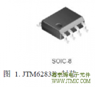 JTM6283B是一款升压恒流型
人气:160
JTM6283B是一款升压恒流型
人气:160
 ADF5904 接收器降频转换器
人气:158
ADF5904 接收器降频转换器
人气:158
 JM100支持 QC2.0 协议的低成
人气:132
JM100支持 QC2.0 协议的低成
人气:132
 自动补偿输入电压,电感
人气:131
自动补偿输入电压,电感
人气:131
 粤ICP备13004986号-3