

1.产品概述 2.产品特点
3.应用范围 4.产品封装图
5.电路原理图 6.产品PCB
7.产品BOM 8.产品PDF文档
9.功能概述
一,产品概述(General Description)
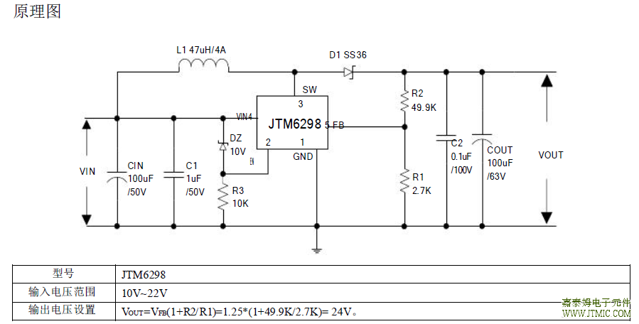
221024A01 是为产品 JTM6298 制作的演示板,用于 DC10~22V 输入,输出 24V,输出最大 0.8A 的应用演示,最高转换效率可以达到 94%以上。
JTM6298 是开关升降压型 DC-DC 转换芯片;固定开关频率 400KHz,可减小外部元器件尺寸。芯片具有出色的线性调整率与负载调整率,最大输出电压支持可达 60V。芯片内部集成过流保护、过温保护、SW 过压保护等可靠性模块。
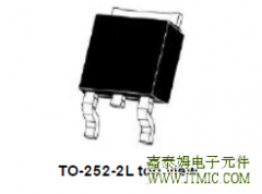
JTM6298 为 TO252-5L 封装,采用标准外部元器件,应用灵活
二.产品特点(Features)
Wide 3.6V to 32V Input Voltage Range
Positive or Negative Output Voltage
Programming with a Single Feedback Pin
Current Mode Control Provides Excellent
Transient Response
1.25V reference adjustable version
Fixed 400KHz Switching Frequency
Maximum 3A Switching Current
SW PIN Built in Over Voltage Protection
Excellent line and load regulation
EN PIN TTL shutdown capability
Internal Optimize Power MOSFET
High efficiency up to 92%
Built in Frequency Compensation
Built in Soft-Start Function
Built in Thermal Shutdown Function
Built in Current Limit Function
Available in TO252-5L package
三,应用范围 (Applications)
1.Automotive and Industrial Boost Buck-Boost / Inverting Convertersn
2.Portable Electronic Equipment
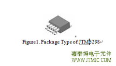
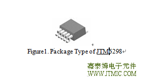
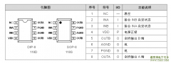
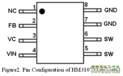
四,产品封装图 (Package)
五,电路原理图
六, 产品PCB
(略)
七.产品BOM
| Item | Qty | Ref Des | Description | Mfg Part Number | Mfg |
| 1 | 1 | C1 | 1uF,50V,Ceramic,X7R,0805 | C2012X7R1H105K | TDK |
| 2 | 1 | C2 | 0.1uF,100V,Ceramic,X7R,0805 | C2012X7R1H104K | TDK |
| 3 | 1 | Cin | 100uF,50V,Electrolytic | YXJ-50V-100uF | Rubycon |
| 4 | 1 | Cout | 100uF,63V,Electrolytic | YXJ-63V-100uF | Rubycon |
| 5 | 1 | D1 | 60V,3A,Schottky Rectifier,SMC | SS36 | Fairchild |
| 6 | 1 | DZ | 10V,500mA,Zener,MINI MELE | ZMM55C10 | ICM |
| 7 | 1 | L1 | 47uH,4A,Toroidal,13*7 | ||
| 8 | 1 | R1 | 2.7KΩ,1%,1/16W,Thick Film,0603 | RL0603xR-072701L | Yageo |
| 9 | 1 | R2 | 49.9KΩ,1%,1/16W,Thick Film,0603 | RL0603xR-074992L | Yageo |
| 10 | 1 | R3 | 10 KΩ,1%,1/16W,Thick Film,0603 | RL0603xR-071002L | Yageo |
| 11 | 1 | U1 | BOOST DC-DC Converter,TO252-5L | JTM6298 | H&M SEMI |
八.产品PDF文档
 |
JTM6298 是开关升降压型 DC-DC 转换芯片 |
九,功能概述
Absolute Maximum Ratings
| Parameter | Symbol | Value | Unit |
| Input Voltage | Vin | -0.3 to 36 | V |
| Feedback Pin Voltage | VFB | -0.3 to Vin | V |
| EN Pin Voltage | VEN | -0.3 to Vin | V |
| Output Switch Pin Voltage | VOutput | -0.3 to 60 | V |
| Power Dissipation | PD | Internally limited | mW |
|
Thermal Resistance (TO252-5L) (Junction to Ambient, No Heatsink, Free Air) |
RJA | 50 | ºC/W |
| Operating Junction Temperature | TJ | -40 to 125 | ºC |
| Storage Temperature | TSTG | -65 to 150 | ºC |
| Lead Temperature (Soldering, 10 sec) | TLEAD | 260 | ºC |
| ESD (HBM) | >2000 | V |
Electrical Characteristics (DC Parameters)
Vin = 12V, GND=0V, Vin & GND parallel connect a 220uf/50V capacitor; Iout=0.5A, Ta =
25℃; the others floating unless otherwise specified.
| Parameters | Symbol | Test Condition | Min. | Typ. | Max. | Unit |
| Input operation voltage | Vin | 3.6 | 32 | V | ||
| Shutdown Supply Current | ISTBY | VEN=0V | 70 | 100 | uA | |
| Quiescent Supply Current | Iq |
VEN =2V, VFB =Vin |
2.5 | 5 | mA | |
| Oscillator Frequency | Fosc | 320 | 400 | 480 | Khz | |
| Switch Current Limit | IL | VFB =0 | 3 | A | ||
| Output Power NMOS | Rdson |
Vin=12V, ISW=3A |
110 | 120 | mohm | |
| EN Pin Threshold | VEN |
High (Regulator ON) Low (Regulator OFF) |
1.4 0.8 |
V | ||
|
EN Pin Input Leakage Current |
IH | VEN =2V (ON) | 3 | 10 | uA | |
| IL | VEN =0V (OFF) | 3 | 10 | uA | ||
| Max. Duty Cycle | DMAX | VFB=0V | 90 | % |
 HM3105B DC-DC 转换芯片;固
人气:367
HM3105B DC-DC 转换芯片;固
人气:367
 1.5A 同步移动电源方案JT
人气:218
1.5A 同步移动电源方案JT
人气:218
 JTM5901用于移动电源的管理
人气:199
JTM5901用于移动电源的管理
人气:199
 JTM118 ,JTM117单通道直流马达
人气:158
JTM118 ,JTM117单通道直流马达
人气:158
 The JTM60N06K uses advanced tre
人气:109
The JTM60N06K uses advanced tre
人气:109
 JTM3107C用于DC16V~90V 输入,
人气:92
JTM3107C用于DC16V~90V 输入,
人气:92
 JTM2518 有刷直流马达驱动
人气:75
JTM2518 有刷直流马达驱动
人气:75
 JTM2528,JTM2522 双通道直流马
人气:70
JTM2528,JTM2522 双通道直流马
人气:70
 粤ICP备13004986号-3