|
目录
一,产品概述(General Description) The JTMX1410 is a 380KHz fixed frequency PWM buck (step-down) DC/DC converter,capable of driving a 2A load with high efficiency, low ripple and excellent line and load regulation. Requiring a minimum number of external components, the regulator is simple to use and include internal frequency compensation and a fixed-frequency oscillator. The PWM control circuit is able to adjust the duty ratio linearly from 0 to 100%. An enable function, an over current protection function is built inside. When short protection function happens, the operation frequency will be reduced from 380KHz to 80KHz. An internal compensation block is built in to minimize external component count. 二.产品特点(Features) Wide 3.6V to 18V Input Voltage Range Output Adjustable from 1.222V to 16V Maximum Duty Cycle 100% Minimum Drop Out 0.6V Fixed 380KHz Switching Frequency 2A Constant Output Current Capability Internal Optimize Power MOSFET High efficiency Excellent line and load regulation TTL shutdown capability EN pin with hysteresis function Built in thermal shutdown function Built in current limit function Built in output short protection function Available in SOP8L package 三,应用范围 (Applications) LCD Monitor and LCD TV Digital Photo Frame Set-up Box ADSL Modem Telecom / Networking Equipment 四.技术规格书下载(产品PDF)
五,产品封装图 (Package) 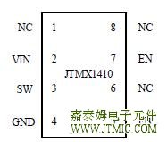 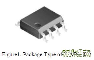
 七,功能概述
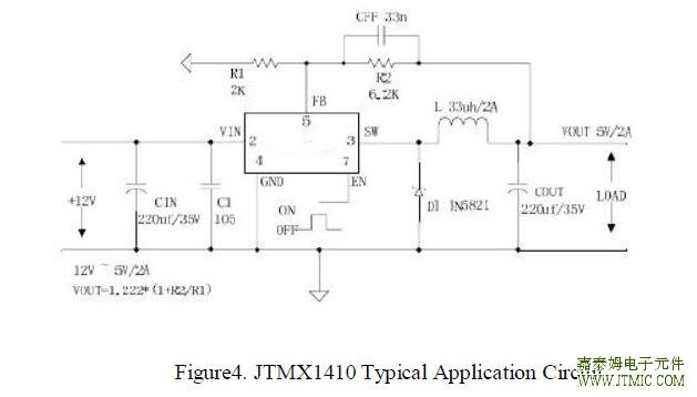
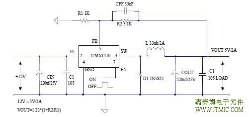
八.JTMX1410 DEMO BOARD MANUAL (一)JTMX1410 典型应用测试:
 2. JTMX1410 12V 转 5V(负载 0.2A—2A)效率图和输出电压变化曲线:  (二)JTMX1410 PCB 板布局建议: (1)流大电流的线要粗,短,不拐弯。 (2)4 脚(GND),2 脚(VIN)线要粗,短线,不拐弯,且输入电解电容 CIN 和 105 C1 陶 瓷电容紧挨第 2 脚(VIN)和 4 脚(GND)。(主要是为了减小输入电源布线寄生的电感,电阻 产生的高压开关毛刺干扰) (3)3 脚(SW)输出线要粗,短线,不拐弯,电感和续流二极管要紧挨第 3 脚(SW)输出 端。 (4)5 脚(FB)走线要接到输出滤波电容 C2,COUT 之后, PCB 布线远离 L1,D1,避免噪声干扰。 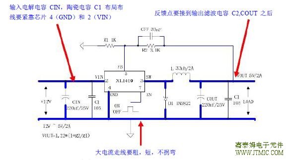 JTMX1410PCB 图: 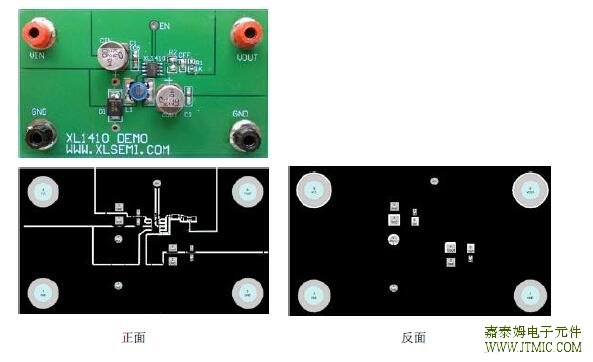 (三)JTMX1410 温度测试数据: 1:JTMX1410 电路图和 PCB 版图。 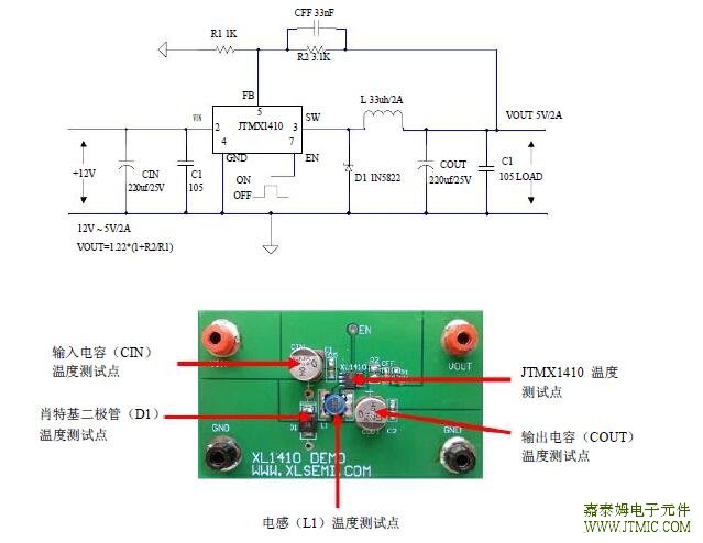 2:JTMX1410 DEMO 板工作时(12V 转 5V)各元件温度,自然通风,室温:16℃。
(责任编辑:oumao18) |


 粤ICP备13004986号-3