JTM4583A is a wide input voltage, high efficiency CC step-
时间:2015-09-06 12:11来源:未知 作者:oumao18 点击:
次
目录 1. 产品概述 2. 产品特点 3. 应用范围 4. 产品封装图 5. 电路原理图 6. 产品PCB 7. 产品BOM 8. 产品PDF文档 9. 功能概述 10 . 相关产品 一 , 产品概述( General Description) JTM4583A is a wide input voltage, hig
|
目录
一,产品概述(General Description)
JTM4583A is a wide input voltage, high efficiency CC step-down DC/DC converter that operates in either CV (Constant Output Voltage) mode or CC (Constant Output Current) mode. JTM4583A provides up to 3.5A output current at 125kHz switching frequency.
JTM4583A provides OVP pin for output over voltage protection.Protection features include cycle-by-cycle current limit, thermal shutdown, and frequency foldback at short circuit. The devices are available in a SOP-8EP package and require very few external devices for operation.
二.产品特点(Features)
42V Input Voltage Surge
40V Steady State Operation
Up to 3.5A output current
Output Voltage 2.5V to 10V
Resistor Programmable
− Current Limit from 1.5A to 3.5A
− Cable Compensation from 0Ω to 0.4Ω
±7.5% CC Accuracy
− Compensation of Input /Output Voltage Change
− Temperature Compensation
2% Feedback Voltage Accuracy
Up to 94% Efficiency
125kHz Switching Frequency Eases EMI Design
Advanced Feature Set
− Integrated Soft Start
− Thermal Shutdown
− Protection Against Shorted ISET Pin
Patented E-LTI technology improves
transient response.
SOP-8EP Package
Long -waiting-time hiccup mode
三,应用范围 (Applications)
Car Charger/ Adaptor
Rechargeable Portable Devices
General-Purpose CC/CV Supply
四,产品封装图 (Package)
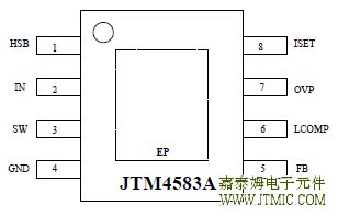
Pin
No. |
NAME |
Description |
|
1 |
HSB |
High Side Bias Pin. This provides power to the internal high-side MOSFET gate driver.
Connect a 100nF capacitor from HSB pin to SW pin. |
|
2 |
IN |
Power Supply Input. Bypass this pin with a 10µF ceramic capacitor to GND, placed as
close to the IC as possible. |
|
3 |
SW |
Power Switching Output to External Inductor. |
|
4 |
GND |
Ground. Connect this pin to a large PCB copper area for best heat dissipation. Return FB,
COMP, and ISET to this GND, and connect this GND to power GND at a single point for
best noise immunity. |
|
5 |
FB |
Feedback Input. The voltage at this pin is regulated to 0.800V. Connect to the resistor
divider between output and GND to set the output voltage. |
|
6 |
LCOMP |
Output cable resistance compensation. |
|
7 |
OVP/EN |
HM4583A: OVP input. If the voltage at this pin exceeds 1.25V, the IC shuts down high
-side switch.
HM4583B: EN input. If the voltage at this pin is below 1.5V, the IC remains shut-off. |
|
8 |
ISET |
Output Current Setting Pin. Connect a resistor from ISET to GND to program the output
current. |
|
|
Exposed
Pad |
Heat Dissipation Pad. Connect this exposed pad to large ground copper area with copper
and vias. |
(责任编辑:oumao18) |
------分隔线----------------------------

 粤ICP备13004986号-3