|
目录
一,产品概述(General Description) The JTM4523 is a wide input voltage high-efficiency Step-down DC/DC converter that operates in either CV (Constant Output Voltage) mode or CC (Constant Output Current) mode. JTM4523 provides up to 3A output current at 225-KHz switching frequency eases EMI design. Integrated sensor-less CC control scheme of the JTM4523 eliminates the expensive, high accuracy current sense resistor, making it ideal for battery charging applications and adaptors with accurate current limit. The JTM4523 achieves higher efficiency than traditional constant current switching regulators by eliminating its associated power loss. Protection features include cycle-by-cycle current limit, thermal shut-down, and frequency foldback at shot circuit. The devices are available in a SOP- 8EP package and require very few external devices for operation. 二.产品特点(Features)
10V to 36V Input Voltage
40V Transparent Input Voltage Surge Up to 3A Constant Output Current Output Voltage Up to 15V High efficiency: up to 92% 225KHz Switching Frequency Eases EMI Design Integrated Sensor-less Constant Current (CC) Control Resistor Programmable for Current Limit from 1.5A to 3A 8% CC Accuracy 三,应用范围 (Applications) Car Charger/Adaptor Rechargeable Portable Devices General-Purpose CC/CV Supply 四.下载产品资料PDF文档
五,产品封装图 (Package) 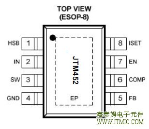
|


 粤ICP备13004986号-3