|
目录
一,产品概述(General Description) The JTMT201XCL/JTMT201XCL series is a synchronous step-down micro DC/DC converter which integrates an inductor and a control IC in one tiny package (2.5mm×2.0mm, h=1.0mm). A stable power supply with an output current of 400mA is configured using only two capacitors connected externally.
Operating voltage range is from 2.0V to 6.0V.
to the VSS level as a result of this functionOutput voltage is internally set in a range from 0.8V to 4.0V in increments of 0.05V. The device is operated by 1.2MHz, and includes 0.42ΩP-channel driver transistor and 0.52ΩN-channel switching transistor. As for operation mode, the JTMT201XCL series is PWM control, the JTMT202XCL series is automatic PWM/PFM switching control, allowing fast response, low ripple and high efficiency over the full range of loads (from light load to heavy load).During stand-by, the device is shutdown to reduce current consumption to as low as 1.0μA or less. With the built-in UVLO (Under Voltage Lock Out) function, the internal driver transistor is forced OFF when input voltage becomes 1.4V or lower.The series provide short-time turn-on by the soft start function internally set in 0.25ms (TYP). The series integrate CL auto discharge function which enables the electric charge stored at the output capacitor CL to be discharged via the internal auto-discharge switch located between the LX and VSS pins. When the devices enter stand-by mode, output voltage quickly returns 二.产品特点(Features)
三,应用范围 (Applications) ●Mobile phones, Smart phones ●Bluetooth Headsets ●WiMAX PDAs, MIDs, UMPCs ●Portable game consoles ●Digital cameras, Camcorders ●SSD(Solid State Drive) ●PND(Portable Navigation Device) 四.技术规格书下载(产品PDF)
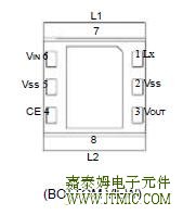 Inductor Electrodes
 七,功能概述
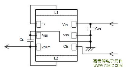
The JTMT201XCL/JTMT202XCL series consists of a reference voltage source, ramp wave circuit, error amplifier,
current for each switching operation, and modulates the error amplifier output signal to provide multiple feedbackPWM comparator, phase compensation circuit, output voltage adjustment resistors, P-channel MOSFET driver transistor, N-channel MOSFET switching transistor for the synchronous switch, current limiter circuit, UVLO circuit with control IC, and an inductor. (See the block diagram below.) Using the error amplifier, the voltage of the internal voltage reference source is compared with the feedback voltage from the VOUT pin through split resistors, R1 and R2. Phase compensation is performed on the resulting error amplifier output, to input a signal to the PWM comparator to determine the turn-on time during PWM operation. The PWM comparator compares, in terms of voltage level, the signal from the error amplifier with the ramp wave from the ramp wave circuit, and delivers the resulting output to the buffer driver circuit to cause the Lx pin to output a switching duty cycle. This process is continuously performed to ensure stable output voltage.The current feedback circuit monitors the P-channel MOS driver transistor signals. This enables a stable feedback loop even when a low ESR capacitor such as a ceramic capacitor is used ensuring stable output voltage 八,相关芯片选择指南
(责任编辑:oumao18) |
|||||||||||||||||||||||||||||||||||||||||||||||||||||||||||||||||||||||||||||||||||||||||||||||||||||||||||||||||||||||||||||||||||||||||||||||||||||||||||||||||||||||||||||||||||||||||||||||||||


 粤ICP备13004986号-3