|
目录
一,产品概述(General Description) The JTMA1280AMP is a simple, cost-effective and high-speed linear regulator designed to generate termination voltage in double data rate (DDR) memory system to comply with the JEDEC SSTL_2 and SSTL_18 or other specific interfaces such as HSTL,SCSI-2 and SCSI-3 etc. devices requirements. The regulator is cJTMAable of actively sinking or sourcing up to 2A while regulating an output voltage to within 40mV.The output termination voltage cab be tightly regulated to track 1/2VDDQ by two external voltage divider resistors or the desired output voltage can be pro-grammed by externally forcing the REFEN pin voltage. The JTMA1280AMP also incorporates a high-speed differential amplifier to provide ultra-fast response in line/load transient. Other features include extremely low initial offset voltage, excellent load regulation, current limiting in bi-directions and on-chip thermal shut-down protection.Built-in softstart function avoids a misoperation by inrush current. The JTMA1280AMP are available in the ESOP-8 (Exposed Pad) surface mount packages. 二.产品特点(Features) Ideal for DDR-I, DDR-II and DDR-III VTT JTMAplications Sink and Source up to 2Amp Integrated Power MOSFETs Generates Termination Voltage for SSTL_2, SSTL_18, HSTL, SCSI-2 and SCSI-3 Interfaces. High Accuracy Output Voltage at Full-Load Output Adjustment by Two External Resistors Built-in Soft-start Function Shutdown for Suspend to RAM (STR) Functionality with High-Impedance Output Current Limiting Protection On-Chip Thermal Protection Available in ESOP-8 (Exposed Pad) Packages VIN and VCNTL Under Voltage Protection RoHS Compliant and Halogen Free 三,应用范围 (Applications) Desktop PCs, Notebooks, and Workstations GrJTMAhics Card Memory Termination Set Top Boxes, Digital TVs, Printers Embedded Systems Active Termination Buses DDR-I, DDR-II and DDR-III Memory Systems 四.技术规格书下载(产品PDF)
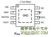 六.电路原理图 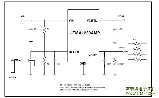 七,功能概述
Input Voltage (VIN) ------------------------------------------ 6V
Lead Temperature (Soldering, 10sec.) ---------------260°CCNTL Pin Voltage (VCNTL) -------------------------------- 6V Power Dissipation (PD) ------------------------------------ Internally Limited Storage Temperature Range (TST) --------------------- -65 to +150°C Thermal Resistance from Junction to Case (R thjc)28°C/W 八,相关芯片选择指南
(责任编辑:oumao18) |
||||||||||||||||||||||||||||||||||||||||||||||||||||||||||||||||||||||||


 粤ICP备13004986号-3