六.电路原理图
七,功能概述
FUNCTIONAL DESCRIPTION
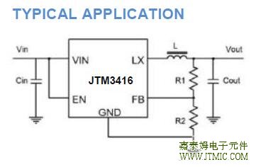
JTM3416 is a synchronous buck regulator IC that integrates the PWM/PFM control, top
and bottom switches on the same die to minimize the switching transition loss and
conduction loss. With ultra low RDS(ON) power switches and proprietary PWM control,
this regulator IC can achieve the highest efficiency and the highest switch frequency
simultaneously to minimize the external inductor and capacitor size, and thus
achieving the minimum solution footprint.The JTM3416 requires only three external
power components (Cin, Cout and L). Theadjustable version can be programmed
with external feedback to any voltage,ranging from 0.6V to the input voltage.
At dropout, the converter duty cycle increases to 100% and the output voltage
tracks the input voltage minus the Rdson drop of the high-side MOSFET.
The internal error amplifier and compensation provides excellent transient response, load,
and line regulation. Soft start function prevents input inrush current and output
overshoot during start up.
Inductor Selection
For most designs, the JTM3416 operates with inductors of 1µH to 4.7µH. Low inductance
values are physically smaller but require faster switching, which results in some efficiency loss.
The inductor value can be derived from the following equation:
L =VIN × ∆I L × f OSC
Where ∆I L is inductor Ripple Current. Large value inductors result in lower ripple current and
small value inductors result in high ripple current. For optimum voltage-positioning load
transients, choose an inductor with DC series resistance in the 50mΩ to 150mΩ range.
Input Capacitor Selection
With the maximum load current at 1.5A, the maximum ripple current through input capacitor
is about 0.6Arms. A typical X7R or better grade ceramic capacitor with 6V rating and greater
than 10uF capacitance can handle this ripple current well. To minimize the potential noise
problem, place this ceramic capacitor really close to the IN and
GND pins. Care should be taken to minimizethe loop area formed by CIN, and IN/GND pins.
Output Capacitor Selection
The output capacitor is required to keep the output voltage ripple small and to ensure
regulation loop stability. The output capacitor must have low impedance at the switching
frequency. Ceramic capacitors with X5R or X7R dielectrics are recommended due to their low
ESR and high ripple current ratings. The outputripple VOUT is determined by:
VOUT × (V IN − VOUT ) 1
V IN × f OSC × L 8 × f osc × C3
A 10µF ceramic can satisfy most applications.PC Board Layout Checklist When laying out the printed
circuit board, the following checking should be used to ensure proper operation of the JTM3416. Check the
following in your layout:
1. The power traces, consisting of the GND trace, the SW trace and the VIN traceshould be kept short,
direct and wide.
2. Does the (+) plates of Cin connect to Vin as closely as possible? This capacitor provides the AC current
to the internal power MOSFETs.
3. Keep the switching node, SW, away from the sensitive VOUT node.
4. Keep the (-) plates of Cin and Cout as close as possible
八,相关产品
|
单N沟道低压MOS场效应管 |
|
型号 |
沟道 |
VDS |
VGS |
VTH |
ID |
IDM |
RDS(on) |
封装 |
状态 |
直接替代型号 |
|
(Max) |
(Max) |
(Max) |
|
JTM2302/A |
N沟道 |
20V |
10V |
0.75V |
3A |
10A |
30mΩ |
SOT23 |
量产 |
Si2302/AP2302/XP151A |
|
SOT23-3L |
APM2314/IRLML2502 |
|
JTM2302B |
N沟道 |
20V |
12V |
0.85V |
2.5A |
10A |
46mΩ |
SOT23 |
量产 |
Si2302/AP2302/XP151A |
|
APM2314/IRLML2502 |
|
JTM2306/A |
N沟道 |
30V |
12V |
0.9V |
5.8A |
22A |
25mΩ |
SOT23 |
量产 |
AP2306/SI2306 |
|
SOT23-3L |
APM2306/WNM2306 |
|
JTM2300/B |
N沟道 |
20V |
12V |
0.65V |
4.5A |
13.5A |
22mΩ |
SOT23 |
量产 |
AP2312/SI2312 |
|
SOT23-3L |
SI2300/AP2300 |
|
JTM2312/B |
N沟道 |
20V |
12V |
0.65V |
4.5A |
13.5A |
22mΩ |
SOT23 |
量产 |
AP2312/SI2312 |
|
SOT23-3L |
SI2300/AP2300 |
|
JTM2314/B |
N沟道 |
20V |
12V |
0.65V |
4.5A |
13.5A |
22mΩ |
SOT23 |
量产 |
AP2314/SI2314 |
|
SOT23-3L |
SI2312/AP2312 |
|
JTM3400/B |
N沟道 |
30V |
12V |
0.9V |
5.8A |
30A |
25mΩ |
SOT23 |
量产 |
AO3400/AO3402/AP2306 |
|
SOT23-3L |
SI2306/APM2306/WNM2306 |
|
JTM3400C |
N沟道 |
30V |
20V |
1.5V |
3.6A |
15A |
40mΩ |
SOT23 |
量产 |
AO3400/AO3402/AO3406/AP2306 |
|
SI2306/APM2306/WNM2306 |
|
JTM3406/B |
N沟道 |
30V |
20V |
1.6V |
5.8A |
20A |
25mΩ |
SOT23 |
量产 |
AO3406/AP2306 |
|
SOT23-3L |
SI2306/APM2306/WNM2306 |
|
JTM3414/B |
N沟道 |
20V |
10V |
0.75V |
3.0A |
10A |
30mΩ |
SOT23 |
量产 |
AO3414 |
|
SOT23-3L |
|
JTM3416E |
N沟道 |
20V |
12V |
0.7V |
6.0A |
30A |
19mΩ |
SOT23-3L |
量产 |
AO3416 |
|
带ESD保护 |
|
JTM3420/B |
N沟道 |
20V |
12V |
0.65V |
4.5A |
13.5A |
22mΩ |
SOT23 |
量产 |
AO3420/SI2300 |
|
SOT23-3L |
SI2312/AP2300 |
|
JTM2318 |
N沟道 |
40V |
20V |
2.0V |
4.0A |
20A |
32mΩ |
SOT23-3L |
量产 |
Si2318 |
|
JTM6400 |
N沟道 |
30V |
12V |
0.9V |
6.9A |
30A |
25mΩ |
SOT23-6L |
量产 |
AO6400/SI3456/AP2602/AO6404 |
|
JTM7002 |
N沟道 |
60V |
20V |
1.7V |
0.115A |
0.8A |
1.3Ω |
SOT23 |
量产 |
2N7002/BSS138/FDV301N |
|
JTM2310 |
N沟道 |
60V |
20V |
1.4V |
3A |
10A |
105mΩ |
SOT23-3L |
量产 |
AP2310GN/APM2360A/AO3422 |
|
IRFL014/UT3N06 |
|
JTM3422 |
N沟道 |
60V |
20V |
1.4V |
3A |
10A |
105mΩ |
SOT23-3L |
量产 |
AO3422/AP2310GN/APM2360A |
|
CES2362/VN3205/VN2204 |
|
IRFL014/UT3N06 |
|
JTM2N10MR |
N沟道 |
100V |
20V |
1.8V |
2A |
5A |
210mΩ |
SOT23-3L |
量产 |
|
|
JTM2324E |
N沟道 |
100V |
20V |
1V |
2.7A |
10A |
140mΩ |
SOT23-3L |
量产 |
Si2324/Si2328 |
|
带ESD保护 |
Si2392/AO3442 |
|
JTM4410 |
N沟道 |
30V |
20V |
1.6V |
10A |
50A |
7.5mΩ |
SOP8 |
量产 |
AO4410/AO4403/APM4410 |
|
CEM4410/AP4410/FDS4410 |
|
IRF7832/IRF7805Z |
|
JTM4412 |
N沟道 |
30V |
20V |
1.0V |
7A |
30A |
22mΩ |
SOP8 |
量产 |
AO4412/APM4412/CEM4412 |
|
AP4412/FDS4412/AO4414/ME4414 |
|
JTM4430 |
N沟道 |
30V |
20V |
1.6V |
18A |
50A |
7.5mΩ |
SOP8 |
量产 |
AO4430/APM4430/CEM4430 |
|
AP4430/FDS4430/SI4166 |
|
JTM4480 |
N沟道 |
40V |
20V |
2.0V |
20A |
50A |
16mΩ |
SOP8 |
量产 |
AO4480/AO4240/IRF7842 |
|
Si4840BDY/Si4124DY |
|
JTM4440 |
N沟道 |
60V |
20V |
2V |
4.5A |
20A |
45mΩ |
SOP8 |
量产 |
AO4440/AP9971/STS5NF60L |
|
JTM4486E |
N沟道 |
100V |
20V |
2V |
3.5A |
20A |
85mΩ |
SOP8 |
量产 |
AO4486 |
|
带ESD保护 |
|
JTM4488 |
N沟道 |
150V |
20V |
3.2V |
5.2A |
42A |
31mΩ |
SOP8 |
量产 |
AO4488 |
|
JTM4490 |
N沟道 |
200V |
20V |
3.0V |
3.9A |
30A |
56mΩ |
SOP8 |
量产 |
AO4490 |
|
|
|
|
|
|
|
|
|
|
|
|
|
双N沟道低压MOS场效应管 |
|
|
|
|
|
|
|
|
|
|
|
|
|
|
|
|
|
|
|
|
|
|
型号 |
沟道 |
VDS |
VGS |
VTH |
ID |
IDM |
RDS(on) |
封装 |
状态 |
直接替代型号 |
|
(Max) |
(Max) |
(Max) |
|
JTM4812 |
双N沟道 |
30V |
20V |
1.6V |
7A |
30A |
25mΩ |
SOP8 |
量产 |
AO4812/AO4800 |
|
APM4812/APM4800/ME4812 |
|
JTM4822 |
双N沟道 |
30V |
20V |
1.8V |
8A |
30A |
18mΩ |
SOP8 |
量产 |
AO4822/APM4822/CEM4822 |
|
AP4822/FDS4822 |
|
JTM4828 |
双N沟道 |
60V |
20V |
2V |
4.5A |
20A |
45mΩ |
SOP8 |
量产 |
AO4828/AO4946/APM4946 |
|
AP4946/FDS4946 |
|
STM6930/FDS6912A |
|
JTM4886E |
双N沟道 |
100V |
20V |
2V |
3.5A |
20A |
85mΩ |
SOP8 |
量产 |
AO4886 |
|
带ESD保护 |
|
JTM9926 |
双N沟道 |
20V |
10V |
0.9V |
5A |
24A |
23mΩ |
SOP8 |
量产 |
AO9926/CEM9926/APM9926 |
|
AP9926/AO8822/AO8810 |
|
JTM8205 |
双N沟道 |
19.5V |
10V |
0.7V |
4A |
16A |
21mΩ |
SOT-26 |
量产 |
AO8205/CEM8205 |
|
APM8205/AP8205 |
|
JTM8205A |
双N沟道 |
19.5V |
10V |
0.7V |
6A |
25A |
21mΩ |
TSSOP8 |
量产 |
AO8205A/CEM8205 |
|
APM8205/AP8205 |
|
JTM8205B |
双N沟道 |
20V |
10V |
0.65V |
4A/6A |
16A |
24mΩ |
SOT-26 |
量产 |
AO8205/CEM8205 |
|
APM8205/AP8205 |
|
JTM8810E |
双N沟道 |
20V |
12V |
0.7V |
7A |
30A |
15mΩ |
SOT-26 |
量产 |
AO8810/AO8820/AO8822 |
|
带ESD保护 |
TSSOP8 |
SSF2418E/SSF2816E |
|
JTM8810B |
双N沟道 |
20V |
12V |
0.7V |
7A |
30A |
15mΩ |
TSSOP8 |
量产 |
AO8808/AO8808A |
|
带ESD保护 |
|
不共D |
|
JTM8820E |
双N沟道 |
20V |
12V |
0.7V |
7A |
30A |
15mΩ |
TSSOP8 |
量产 |
AO8820/AO8810/AO8822 |
|
带ESD保护 |
SSF2418E/SSF2816E |
|
JTM8822E |
双N沟道 |
20V |
12V |
0.7V |
7A |
30A |
15mΩ |
TSSOP8 |
量产 |
AO8822/AO8810/AO8820 |
|
带ESD保护 |
SSF2418E/SSF2816E |
|
JTM6800 |
双N沟道 |
30V |
12V |
0.9V |
5.8A |
30A |
25mΩ |
SOT-26 |
量产 |
AO6800/AO6802 |
|
AO6804A/AO6810 |
|
|
|
|
|
|
|
|
|
|
|
|
|
|
|
|
|
|
|
|
|
|
|
|
|
N+P沟道低压MOS场效应管 |
|
|
|
|
|
|
|
|
|
|
|
|
|
|
|
|
|
|
|
|
|
|
型号 |
沟道 |
VDS |
VGS |
VTH |
ID |
IDM |
RDS(on) |
封装 |
状态 |
直接替代型号 |
|
(Max) |
(Max) |
(Max) |
|
JTM4606 |
N+P沟道 |
30V/-30V |
20V/-20V |
1.4V/ |
6.5A/ |
28A/ |
23mΩ/ |
SOP8 |
量产 |
AO4606/AO4603/AO4604/ |
|
-1.5V |
-6A |
-26A |
27mΩ |
AP4503/AP4501/STM8401 |
|
JTM4616 |
N+P沟道 |
30V/-30V |
20V/-20V |
1.6V/ |
10.5A/ |
30A/ |
7.5mΩ/ |
SOP8 |
量产 |
AO4616/AO4606/AO4603/ |
|
-1.5V |
-9.1A |
-30A |
15mΩ |
AP4604/AP4503/STM8401 |
|
JTM4611 |
N+P沟道 |
60V/-55V |
20V/-20V |
2.0V/ |
4.5A/ |
20A/ |
45mΩ/ |
SOP8 |
量产 |
AO4611/AO4612/AO4614 |
|
-2.6V |
-5.0A |
-25A |
64mΩ |
|
JTM6602 |
N+P沟道 |
30V/-30V |
12V/-20V |
0.9V/ |
5.8A/ |
30A/ |
25mΩ/ |
SOT23-6L |
量产 |
AO6602/AO6604/SI3552 |
|
-1.0V |
-4.2A |
-30A |
50mΩ |
FDC6333/FDC6327/FDC6420 |
|
|
|
|
|
|
|
|
|
|
|
|
|
|
|
|
|
|
|
|
|
|
|
|
|
|
|
|
|
|
|
|
|
|
|
|
|
|
|
|
|
|
|
|
|
|
|
|
|
|
|
|
|
|
|
|
|
|
|
|
|
|
|
|
|
|
|
|
|
|
|
|
|
|
|
|
|
|
|
|
|
|
|
|
|
|
|
|
|
|
|
|
|
|
|
|
|
|
|
|
|
|
|
|
|
|
|
|
|
|
|
|
|
|
|
|
|
|
|
|
|
|
|
|
|
|
|
|
|
|
|
|
|
备注: |
|
|
|
|
|
|
|
|
|
|
1. 标注的Id电流是MOS芯片的最大常态电流,实际使用时的最大常态电流还要受封装的最大电流限制。因此客户设计产品时的最大使用电流设定要考虑封装的最大电流限制。建议客户设计产品时的最大使用电流设定更重要的是要考虑MOS的内阻参数。 |
|
2. 建议在MOS的栅源(G/S)极之间并一个电阻(10K)和一个稳压二极管(5V-12V)起到保护栅源(G/S)极过压的作用。 |
|
3.建议MOS管的开启电压尽量提高,这样MOS管才能充分开启导通,这个时候内阻最小,不容易发烫。一般建议低压MOS的VGS开启电压设定为4.5V以上,中高压MOS的开启电压设定为10V以上. |
|
4.MOS 电路操作注意事项: |
|
|
|
|
|
|
|
|
|
静电在很多地方都会产生,采取下面的预防措施,可以有效防止MOS 电路由于受静电放电影响而引起的损坏: |
|
• 操作人员要通过防静电腕带接地。 |
|
|
|
|
|
|
|
|
• 设备外壳必须接地。 |
|
|
|
|
|
|
|
|
|
• 装配过程中使用的工具必须接地。 |
|
|
|
|
|
|
|
|
• 必须采用导体包装或抗静电材料包装或运输 |
|
|
|
|
|
|
|
|
|
|
|
|
|
|
|
|
|
|
我司的JTM2301/SOT-23/3A/20V/PMOS的优点:是足3A的电流,内阻小,和市场低端的1A的产品不同,可以用于移动电源/充电器/多节保护板/家电/航模/遥控玩具等大电流/低内阻的应用场合。 |
|
|
|
|
|
|
|
|
|
|
|
|
|
我司的JTM2302/SOT-23/3A/20V/NMOS的优点:是足3A的电流,内阻小,和市场低端的1A的产品不同,可以用于移动电源/充电器/多节保护板/家电/航模/遥控玩具等大电流/低内阻的应用场合。 |
|
|
|
|
|
|
|
|
|
|
|
|
|
我司的JTM3400/SOT-23-3L/5.8A/30V/NMOS的优点:是足5.8A的电流/大SOT-23封装的,内阻小,和市场低端的小SOT-23的不同,可以用于移动电源/充电器/多节保护板/家电/航模/遥控玩具等大电流/低内阻的应用场合。 |
|
|
|
|
|
|
|
|
|
|
|
|
|
我司的JTM3401/SOT-23-3L/4.2A/30V/PMOS的优点:是足4.2A的电流/大SOT-23封装的,内阻小,和市场低端的小SOT-23的不同,可以用于移动电源/充电器/多节保护板/家电/航模/遥控玩具等大电流/低内阻的应用场合。 |
|
|
|
|
|
|
|
|
|
|
|
|
|
我司的JTM2310/SOT-23-3L/3A/60V/NMOS的优点:1.耐压可达60V,足3A电流,大SOT-23封装的。2.可以用于LED照明等耐压高的产品应用。 |
|
|
|
|
|
|
|
|
|
|
|
|
|
我司的JTM4953的优点:电流大内阻小,可以用于全彩屏市场。 |
|
|
|
|
|
|
|
|
|
|
|
|
|
|
|
|
|
|
我司的JTM4430的优点:电流大内阻小,电流可达18A.目前市场上SOP8/NMOS电流最大的一款产品之一。 |
|
|
|
|
|
|
|
|
|
|
|
|
|
|
|
我司的JTM4440的优点:耐压可达60V, 目前市场上SOP8/NMOS耐压最大的一款产品之一。 |
|
|
|
|
|
|
|
|
|
|
|
|
|
|
|
|
|
JTM8810E/SOT-26&TSSOP8/7A/20V/双NMOS的优点:足7A的电流,带ESD静电保护,相比市场上的8205,电流更大内阻更小,可直接替换AO8810/AO8820/AO8822/SSF2418E/SSF2816E,主要可用于高端的锂电保护板/手机电池/多节保护板/移动电源/充电器/家电/航模/遥控玩具等大电流/低内阻的应用场合。 |
|
|
|
|
|
|
|
|
|
|
|
|
|
|
|
|
|
|
|
|
|
|
|
|
|
产品应用: |
|
|
|
|
|
|
|
|
|
|
1.MP3/MP4/MP5/PMP 播放器 |
|
|
|
|
|
|
|
|
|
2.MID/UMPC |
|
|
|
|
|
|
|
|
|
|
3.GPS/蓝牙耳机 |
|
|
|
|
|
|
|
|
|
|
4.PDVD/车载DVD/汽车音响 |
|
|
|
|
|
|
|
|
|
5.液晶电视/液晶显示器 |
|
|
|
|
|
|
|
|
|
6.移动电源/电子烟 |
|
|
|
|
|
|
|
|
|
|
7.手机电池、锂电池保护板 |
|
|
|
|
|
|
|
|
|
8.LED照明/LED电源 |
|
|
|
|
|
|
|
|
|
|
9.LED显示屏 |
|
10.智能充电器 |
|
11.小家电、家电控制板 |
|
12.电脑主板、显卡 |
(责任编辑:oumao18) |

 粤ICP备13004986号-3