六.电路原理图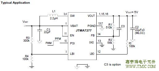 七,功能概述
Main Control Loop
The JTMA7277 is a constant frequency, synchronous rectifier, and current-mode switching regulator. In normal operation, the internal N-channel power MOSFET is turned on each cycle when the oscillator sets an internal RS latch and turned off when an internal comparator (ICMP) resets the latch. The peak inductor current which ICMP resets the RS latch is controlled by the voltage on the COMP node, which is the output of the error amplifier (EAMP). An external resistive divider connected between VOUT and ground allows the EAMP to receive an output feedback voltage VFB at FB pin. When the load current increases, it causes a slightly decrease in VFB relative to the 0.5V reference, which in turn causes the COMP volt- age to increase until the average inductor current matches the new load current. Start-up A start-up oscillator circuit is integrated in the JTMA7277.When the device enables, the circuit pumps the output voltage high. Once the output voltage reaches 1.6V (typ),the main DC-DC circuitry turns on and boosts the output voltage to the final regulation voltage. Automatic PFM/PWM mode Switch The JTMA7277 is a fixed frequency PWM peak current modulation control step-up converter. At light loads, the JTMA7277 will automatically enter in pulse frequency modulation operation to reduce the dominant switching losses. In PFM operation, the inductor current may reach zero or reverse on each pulse. A zero current comparator turns off the P-channel synchronous MOSFET, forcing DCM(Discontinuous Current Mode) operation at light load. These controls get very low quiescent current, help to maintain high efficiency over the complete load range. Synchronous Rectification The internal synchronous rectifier eliminates the need for an external Schottky diode, thus reducing cost and board space. During the cycle off-time, the P-FET turns on and shunts the FET body diode. As a result, the syn- chronous rectifier significantly improves efficiency with-out the addition of an external component. Conversion efficiency can be as high as 92%. Load Disconnect Driving EN to ground places the JTMA7277 in shutdown mode. When in shutdown, the internal power MOSFET turns off, all internal circuitry shuts down and the quies-cent supply current reduces to 1µA maximum. A special circuit is applied to disconnect the load from the input during shutdown the converter. In conventional syn- chronous rectifier circuits, the back-gate diode of the high-side P-FET is forward biased in shutdown and allows current flowing from the battery to the output. However,this device uses a special circuit, which takes the cath- ode of the back-gate diode of the high-side P-FET and disconnects it from the source when the regulator is shutdown. The benefit of this feature for the system de-sign engineer is that the battery is not depleted during shutdown of the converter. No additional componentsmust be added to the design to make sure that the bat- tery is disconnected from the output of the converter. Current-Limit Protection The JTMA7277 monitors the inductor current, flowing through the N-FET, and limits the current peak at current- limit level to prevent loads and the JTMA7277 from dam-ages during overload conditions. Over-Temperature Protection (OTP) The over-temperature circuit limits the junction tempera-ture of the JTMA7277. When the junction temperature ex- ceeds 150oC, a thermal sensor turns off the both N-FETand P-FET, allowing the devices to cool. The thermal sensor allows the converters to start a soft-start process and regulate the output voltage again after the junction temperature cools by 30oC. The OTP is designed with a 30oC hysteresis to lower the average Junction Tempera- ture (TJ) during continuous thermal overload conditions,increasing the lifetime of the device. 八,相关产品
(责任编辑:oumao18) |
|||||||||||||||||||||||||||||||||||||||||||||||||||||||||||||||||||||||||||||||||||||||||||||||||||||||||||||||||||||||||||||||||||||||

 粤ICP备13004986号-3