
BOOT (Pin 1)
This pin provides ground referenced bias voltage to the high-side MOSFET driver. A bootstrap circuit witha diode connected to 5~12V is used to create a voltage suitable to drive a logic-level N-channel MOSFET. UGATE (Pin 2) Connect this pin to the high-side N-channel MOSFET’s gate. This pin provides gate drive for the high-side MOSFET. GND (Pin 3) The GND terminal provides return path for the IC’s biascurrent and the low-side MOSFET driver’s pull-low current. Connect the pin to the system ground via very low impedance layout on PCBs. LGATE (Pin 4) Connect this pin to the low-side N-channel MOSFET’s gate. This pin provides gate drive for the low-side MOSFET. VCC (Pin 5) Connect this pin to a 5~12V supply voltage. This pin provides bias supply for the control circuitry and the low-side MOSFET driver. The voltage at this pin is monitored for the Power-On-Reset (POR) purpose. FB (Pin 6) This pin is the inverting input of the internal Gm amplifier.Connect this pin to the output (VOUT) of the converter via an external resistor divider for closed-loop operation.The output voltage set by the resistor divider is deter- mined using the following formula : where R1 is the resistor connected from VOUT to FB ,and R2 is the resistor connected from FB to GND. The FB pin is also monitored for under and over-voltage events. OCSET (Pin 7) The OCSET is a dual-function input pin for over-current protection and shutdown control. Connect a resistor (ROCSET) from this pin to the Drain of the low-side MOSFET. This resistor, an internal 40µA current source (IOCSET), and the MOSFET’s on-resistance(RDSON) set the converter over-current trip level (IPEAK) according to the following formula: Pulling and holding this pin below 0.15V with an open drain device, with very low parasitic capacitor, shuts down the IC with floating output and also resets the over-current counter. Releasing OCSET pin initiates a new soft-start and the converter works again. PHASE (Pin 8) The pin provides return path for the high-side MOSFETdriver’s pull-low current. Connect this pin to the high- side MOSFET’s source. 六.电路原理图 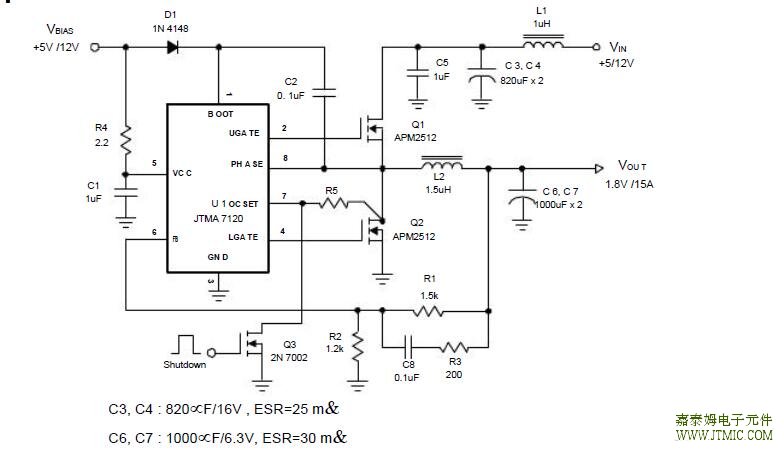 七,功能概述 Power-On-Reset (POR) The JTMA7120 monitors the VCC voltage (V CC) for Power-On-Reset function, preventing wrong logic operation during powering on. When the VCC voltage is ready, the JTMA7120 starts a start-up process and then ramps the output voltage up to the target voltage. Soft-Start The JTMA7120 has a built-in digital soft-start to control the output voltage rise and limit the current surge at the start-up. During the soft-start, an internal ramp con-nected to the one of the positive inputs of the Gm amplifier rises up from 0V to 2V to replace the reference voltage (0.8V) until the ramp voltage reaches the refer- ence voltage. The soft-start interval is about 3.2mstypical, independent of the converter’s input and out- put voltages. Over-Current Protection (OCP) The over-current function protects the switching c o nverter against over-current or short-circuit conditions. The controller senses the inductor current by detecting the drain-to-source voltage, product of the inductor’s current and the on-resistance, of the low-side MOSFET during it’s on-state. This method enhances the converter’s efficiency and reduces cost by eliminating a current sensing resistor. A resistor (ROCSET), connected from the OCSET to the Over-Current Protection (OCP) (Cont.) low-side MOSFET’s drain, programs the over-current trip level. An internal 40µA (typical) current source flowing through the ROCSET develops a voltage (VROCSET) across the ROCSET. When the VOCSET (VROCSET+ VDS of (责任编辑:oumao18) |

 粤ICP备13004986号-3