|
目录
一,产品概述(General Description)
The jtm9266 is a compact, high efficiency, and low voltage step-upDC/DC converter with an Adaptive Current Mode PWM control loop, includes an error amplifier, ramp generator, comparator, switch pass element and driver in which providing a stable and high efficient operation over a wide range of load currents.
It operates in stable waveforms without external compensation.The low start-up input voltage below 1V makes jtm9266 suitable for 1 to 4 battery cells applications of providing up to 300mA output current. The 450KHz high switching rate minimized the size of external components. Besides, the 17µA low quiescent current together with high efficiency maintains long battery lifetime. The output voltage is set with two external resistors. Both internal 2A switch and driver for driving external power devices (NMOS or NPN) are provided. 二.产品特点(Features) 1.0V Low Start-up Input Voltage High Supply Capability to Deliver 3.3V 100mA with 1 Alkaline Cell 17uA Quiescent (Switch-off) Supply Current Zero Shutdown Mode Supply Current 90% Efficiency 450kHz Fixed Switching Frequency Providing Flexibility for Using Internal and External Power Switches Small SOT-26 , SOT89-5 Package 三,应用范围 (Applications)
PDA
RF-TagsDSC LCD Panel MP3 Portable Instrument Wireless Equipment 四.下载产品资料PDF文档
五,产品封装图 (Package) 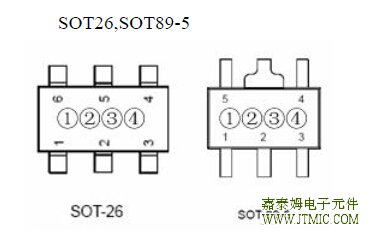 六.电路原理图 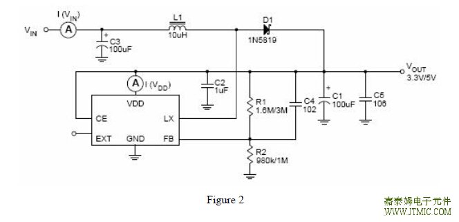 七,功能概述
|


 粤ICP备13004986号-3