|
目录
一,产品概述(General Description) The JTM3103 is a 180 KHz fixed frequency PWM buck (step-down) DC/DC converter,capable of driving a 4A load with high efficiency, low ripple and excellent line and load regulation.Requiring a minimumnumber of external components, the regulator is simple to use and include internal frequency compensation and a fixed-frequency oscillator. The PWM control circuit is able to adjust the duty ratio linearly from 0 to 100%. An over current protection function is built inside.When short protection function happens, the operation frequency will be reduced from 180KHz to 48KHz. An internal compensation block is built in to minimize external component count. 二.产品特点(Features) 1.)Wide 8V to 36V Input Voltage Range 2.)Output Adjustable from 1.25V to 32V 3.)Maximum Duty Cycle 100% 4.)Minimum Drop Out 0.3V 5.)Fixed 180KHz Switching Frequency 6.)4A Constant Output Current Capability 7.)Internal Optimize Power MOSFET 8.)High efficiency 9.)Excellent line and load regulation 10.)Built in thermal shutdown function 11.)Built in current limit function 12.)Built in output short protection function 13.)Available in TO-252 package 三,应用范围 (Applications) LCD Monitor and LCD TV Portable instrument power supply Telecom / Networking Equipment 四.下载产品资料PDF文档
五,产品封装图 (Package) 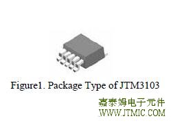 
|


 粤ICP备13004986号-3